Nano-cavity laser of molecule-doped thin film layer with electroexcitation
An electro-excitation, thin-film layer technology, applied in the field of lasers, can solve the problems of difficult manufacturing process, high cost, difficulty in electro-excitation, etc.
- Summary
- Abstract
- Description
- Claims
- Application Information
AI Technical Summary
Problems solved by technology
Method used
Image
Examples
Embodiment Construction
[0012] The specific implementation manners of the present invention will be described in detail below in conjunction with the accompanying drawings.
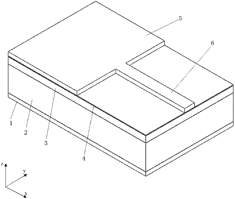
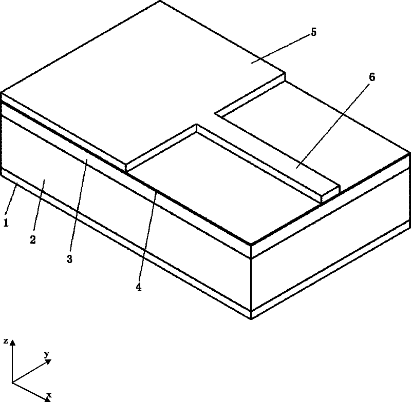
[0013] Such as figure 1 Shown: electro-excited molecule-doped thin-film layer nanocavity laser, including p-face electrode 1, substrate 2, electroluminescence medium 3, molecule-doped thin-film layer 4, n-face electrode 5 and nanowire structure 6; substrate Electroluminescence medium 3, molecular doped thin film layer 4, n-face electrode 5 and nanowire structure 6 are sequentially grown on the top of substrate 2, and p-face electrode 1 is plated on the bottom of substrate 2.
[0014] The molecular doped thin film layer 4 has very little loss to electromagnetic field propagation, the dielectric constant of the thin film layer is smaller than that of the electroluminescent medium, and the ratio d / n of its thickness d to the refractive index n of the thin film layer is less than 50nm, forming a nanocavity structure. The molecules...
PUM
 Abstract
Description
Claims
Application Information
 - R&D
- Intellectual Property
- Life Sciences
- Materials
- Tech Scout
- Unparalleled Data Quality
- Higher Quality Content
- 60% Fewer Hallucinations
Browse by: Latest US Patents, China's latest patents, Technical Efficacy Thesaurus, Application Domain, Technology Topic, Popular Technical Reports.
© 2025 PatSnap. All rights reserved.Legal|Privacy policy|Modern Slavery Act Transparency Statement|Sitemap|About US| Contact US: help@patsnap.com


