Substrate for flexible luminescent device and preparation method thereof
A technology for light-emitting devices and substrates, which is used in the manufacture of semiconductor/solid-state devices, electric solid-state devices, semiconductor devices, etc., and can solve the problems of poor surface flatness of thin-layer carbon nanotubes, poor bonding force between carbon nanotubes and flexible substrates, etc.
- Summary
- Abstract
- Description
- Claims
- Application Information
AI Technical Summary
Problems solved by technology
Method used
Image
Examples
Embodiment 1
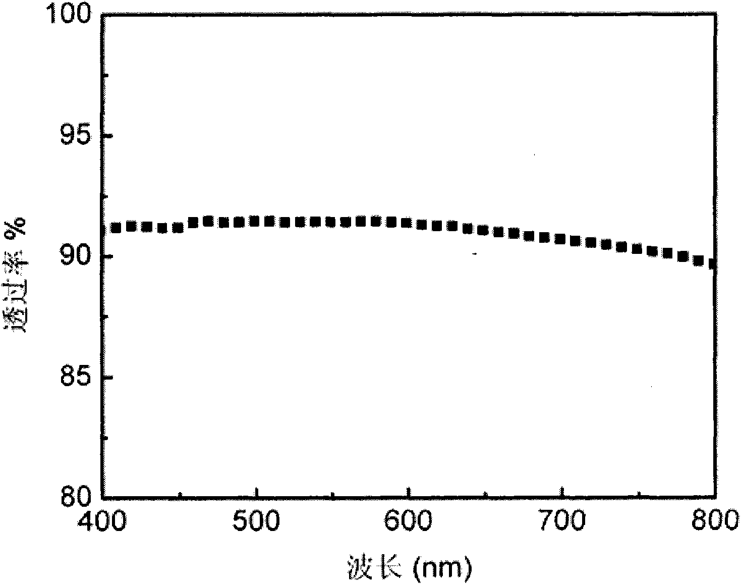
[0099] Such as figure 1 In the substrate structure shown, the flexible substrate 1 uses an adhesive that requires double curing, and the conductive layer 2 uses carbon nanotubes, the gaps of the carbon nanotube layer are filled with organic light-emitting materials, and the thickness of the carbon nanotube layer is 70nm.
[0100] The preparation method is as follows:
[0101] ① Clean the glass substrate with surface roughness less than 1nm, and dry it with dry nitrogen after cleaning;
[0102] ② Evenly disperse carbon nanotubes in a solvent, and prepare a carbon nanotube layer on a clean substrate by spin coating. The rotation speed of spin coating is 4000 rpm, the duration is 60 seconds, and the film thickness is about 70 nanometers;
[0103] ③ Drop-coat the solution containing organic light-emitting materials on the carbon nanotube layer, place the glass substrate in an environment of 80°C for 30 minutes, remove the remaining solvent in the carbon nanotube layer, and then s...
Embodiment 2
[0111] Such as figure 1 As shown in the substrate structure, the flexible substrate 1 adopts an adhesive that requires double curing, the conductive layer 2 adopts carbon nanotubes, the gaps of the carbon nanotube layer are filled with organic light-emitting materials, and the thickness of the carbon nanotube layer is 60 nm. The adhesive raw materials include the following components:
[0112]
[0113] The preparation method is similar to Example 1.
Embodiment 3
[0115] Such as figure 1 As shown in the substrate structure, the flexible substrate 1 adopts an adhesive that requires double curing, the conductive layer 2 adopts carbon nanotubes, and the gaps of the carbon nanotube layer are filled with organic light-emitting materials, and the thickness of the carbon nanotube layer is 50 nm. The adhesive raw materials include the following components:
[0116]
[0117] The preparation method is similar to Example 1.
PUM
| Property | Measurement | Unit |
|---|---|---|
| Thickness | aaaaa | aaaaa |
| Surface roughness | aaaaa | aaaaa |
| Thickness | aaaaa | aaaaa |
Abstract
Description
Claims
Application Information
 - R&D
- Intellectual Property
- Life Sciences
- Materials
- Tech Scout
- Unparalleled Data Quality
- Higher Quality Content
- 60% Fewer Hallucinations
Browse by: Latest US Patents, China's latest patents, Technical Efficacy Thesaurus, Application Domain, Technology Topic, Popular Technical Reports.
© 2025 PatSnap. All rights reserved.Legal|Privacy policy|Modern Slavery Act Transparency Statement|Sitemap|About US| Contact US: help@patsnap.com


