Method for preparing p-type IIB-VIA family quasi-one-dimensional semiconductor nano material by chemical vapor-deposition in-situ doping
A chemical vapor deposition and in-situ doping technology is applied in the field of preparing p-type doped IIB-VIA group quasi-one-dimensional semiconductor nanomaterials, and achieves the effects of good morphology, high crystal quality and simple process
- Summary
- Abstract
- Description
- Claims
- Application Information
AI Technical Summary
Problems solved by technology
Method used
Image
Examples
Embodiment 1
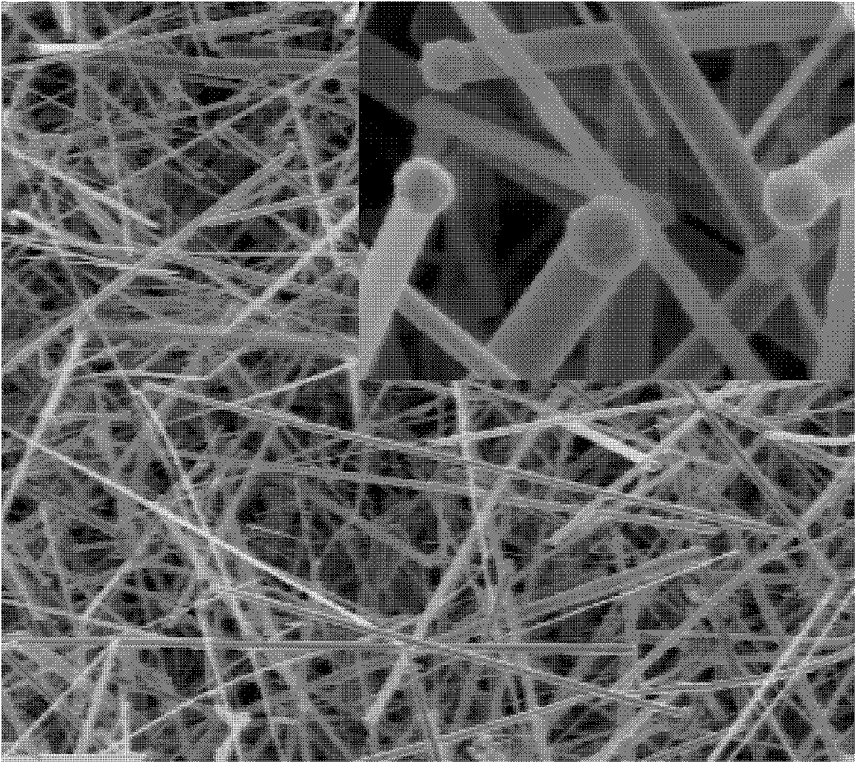
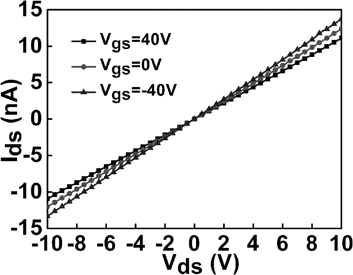
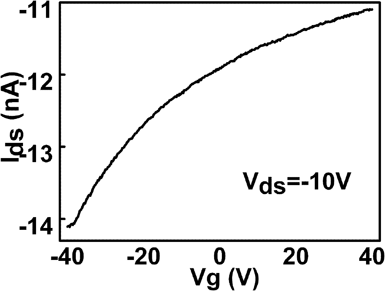
[0027] Put 0.15g of Bi powder with a purity of 99.9% into a porcelain boat and place it on the front of the horizontal tube furnace (5cm away from the heating source), place the porcelain boat with 0.3g of ZnSe powder with a purity of 99.9% in the horizontal tube furnace The heating source inside is the middle part of the horizontal tube furnace, and the evaporated gold silicon wafer used as the deposition substrate is placed at the rear of the horizontal tube furnace (12.5 cm away from the heating source), and the inlet of the argon-hydrogen protective gas flow is As the front of the horizontal tube furnace; seal the furnace body and pump it to a vacuum of 3.0×10 -3 After Pa, argon-hydrogen protective gas is introduced at a rate of 50 SCCM to bring the pressure in the furnace to 20000 Pa, wherein the gas volume ratio of argon and hydrogen is 90-95:10-5. Then raise the temperature to 1000°C, keep it for 1.5h, then cool down the furnace body to room temperature naturally, and u...
Embodiment 2
[0030]Put 0.2g of Sb powder with a purity of 99.9% into a porcelain boat and place it on the front of the horizontal tube furnace (5cm away from the heating source), place the porcelain boat with 0.3g of ZnS powder with a purity of 99.9% in the horizontal tube furnace The heating source inside is the middle part of the horizontal tube furnace, and the evaporated gold silicon wafer used as the deposition substrate is placed at the rear of the horizontal tube furnace (15 cm away from the heating source), and the inlet of the argon-hydrogen protective gas flow is used as the The front of the horizontal tube furnace; seal the furnace body and pump it to a vacuum of 3.0×10 -3 After Pa, argon-hydrogen protective gas is introduced at a rate of 90 SCCM to bring the pressure in the furnace to 20000 Pa, wherein the gas volume ratio of argon and hydrogen is 90-95:10-5. Then raise the temperature to 1100°C, keep it for 1.5h, and then cool down the furnace naturally to room temperature, th...
Embodiment 3
[0033] The porcelain boat that fills the ZnSe powder of 0.3g purity 99.9% is placed on the heating source place in the horizontal tube furnace, that is, the middle part of the horizontal tube furnace, and the evaporated gold silicon wafer used as the deposition substrate is placed in the horizontal tube furnace The rear part of the furnace (10cm away from the heating source), with the inlet of the argon-hydrogen protective gas flow as the front part of the horizontal tube furnace; the furnace body is sealed and evacuated to a vacuum of 3.0×10 -3 After Pa, feed argon-hydrogen protective gas at a rate of 100SCCM, and simultaneously feed ammonia gas at a rate of 8SCCM (the flow ratio of argon-hydrogen protective gas and dopant gas source is 4:50), so that the pressure in the furnace is 20000Pa, of which the argon The gas volume ratio of gas and hydrogen is 90-95:10-5. Then raise the temperature to 1040°C, keep it for 1.5h, and then cool down the furnace naturally to room temperat...
PUM
 Abstract
Description
Claims
Application Information
 - Generate Ideas
- Intellectual Property
- Life Sciences
- Materials
- Tech Scout
- Unparalleled Data Quality
- Higher Quality Content
- 60% Fewer Hallucinations
Browse by: Latest US Patents, China's latest patents, Technical Efficacy Thesaurus, Application Domain, Technology Topic, Popular Technical Reports.
© 2025 PatSnap. All rights reserved.Legal|Privacy policy|Modern Slavery Act Transparency Statement|Sitemap|About US| Contact US: help@patsnap.com


