Preparation method of diode chip on P+ substrate and structure of diode chip

A diode and substrate technology, applied in the field of low-voltage diode chips and its manufacturing, can solve the problems of large leakage of low-voltage diodes and poor voltage uniformity in the chip, and achieve the effect of avoiding lateral breakdown and ensuring voltage uniformity

Active Publication Date: 2011-08-03
CHENGDU SILAN SEMICON MFG
View PDF4 Cites 14 Cited by
  • Summary
  • Abstract
  • Description
  • Claims
  • Application Information

AI Technical Summary

Problems solved by technology

[0006] The purpose of the present invention is in order to overcome the defect in the above-mentioned prior art, has proposed the technical scheme that solves two problems of 2.0V-5.1V low-voltage diode (P+ substrate) electric leakage too large and internal voltage uniformity difference, has proposed a kind of Method and structure for preparing low-voltage diode chip on P+ substrate

Method used


Image

  • Preparation method of diode chip on P+ substrate and structure of diode chip
  • Preparation method of diode chip on P+ substrate and structure of diode chip
  • Preparation method of diode chip on P+ substrate and structure of diode chip

Examples


specific Embodiment approach

[0030] Below in conjunction with accompanying drawing, the present invention is further described, especially with figure 2 For example, the specific implementation method is as follows:

[0031] A kind of method that the present invention proposes prepares low-voltage diode chip on P+ substrate comprises the steps:

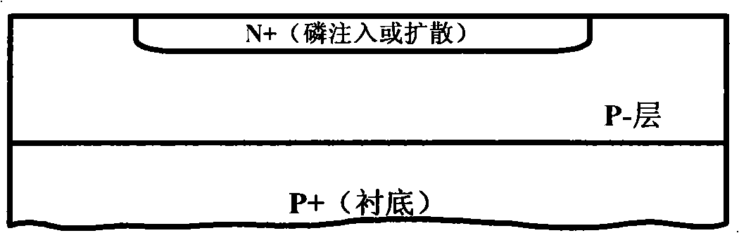
[0032] Step 1: The resistivity of the P+ substrate is about 0.005≤ρ≤0.008Ω.cm, and a P- epitaxial layer with a thickness of 3.0-10.0um and a resistivity of 1.0-5.0Ω.cm is chemically vapor grown at 1050°C.

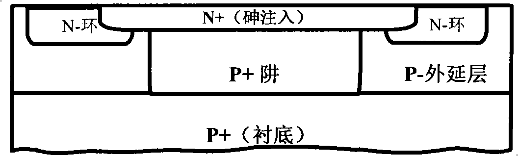
[0033] Step 2: Form an active region by photolithography and etching on the P- epitaxial layer, and then inject boron into the active region to form a P+ well. The dose of the P+ well depends on the breakdown voltage (for low-voltage diodes below 5.1V , the dose is about 1E15-8E15).

[0034] Step 3: P well annealing temperature is 1100°C-1200°C for 1h-2h.

[0035] Step 4: Form the N-ring region by photolithography and etching, and the N-ring dose is relati...


PUM

PropertyMeasurementUnit
electrical resistivityaaaaaaaaaa

Abstract

The invention discloses a preparation method of a diode chip on a P+ substrate and a structure of the diode chip. The method comprises the following steps of: directly forming a P- epitaxial layer on the P+ substrate through epitaxy; forming a P+ well through filling boron; annealing a P well; forming an N- ring region through photoetching and etching; annealing the N- ring; forming an N+ main junction region through photoetching and etching; annealing the N+ main junction region; evaporating or sputtering A1 as a positive electrode and the like. In the structure, special structures of the P-epitaxial layer, the P+ well and an N- voltage dividing ring device, and an N+ arsenic filling process are adopted to ensure that the N+/P+ is broken down on a plane and to avoid lateral breakdown; the voltage of a diode formed on the P+ substrate is reduced to be lower than 5.1V, the lowest voltage can reach 2.0V, and leakage current is within 100uA, so that the uniformity of the voltage in the chip is ensured to be within 5%; and in fact the diode is a P-N junction formed by the P well and an N+ region. The structure is successfully applied to the fields of a low-voltage voltage-regulator diode and a low-voltage transient voltage suppressor diode.

Description

technical field [0001] The invention relates to the field of semiconductor chip manufacturing, in particular to a low-voltage diode chip and a manufacturing method thereof. Background technique [0002] Compared with high-voltage diodes, low-voltage diodes have special requirements on the structure and manufacturing process of the device, which is mainly due to the large leakage of low-voltage diodes. Theoretically, low-voltage diodes are composed of P+ / N+ structures with extremely high concentrations on both sides, which belong to Zener breakdown (also called tunnel breakdown), the breakdown point of the I-V curve is soft, and the reverse leakage is large. Therefore, if N+ is directly injected into a very dense P+ substrate to form a P+ / N+ junction, although the voltage may reach below 5.1V, the leakage will reach the milliampere level, basically unable to form a diode with good performance. See figure 1 , a brief introduction is as follows: [0003] First implant a laye...

Claims


Application Information

Patent Timeline
Patent Type & Authority Applications(China)
IPC IPC(8): H01L21/329H01L21/265H01L29/861H01L29/06
Inventor 张常军王平周琼琼
Owner CHENGDU SILAN SEMICON MFG
Why Eureka
Try Eureka