Force modulation mode-based dip-pen nanolithography method
A modulation mode, nanotechnology, applied in nanotechnology, nanotechnology, nanostructure manufacturing, etc., can solve the problems of time occupied, different, difficult to repeat etching results, etc., to achieve improved repeatability, good etching results, good etching results. Beneficial to industrialization
- Summary
- Abstract
- Description
- Claims
- Application Information
AI Technical Summary
Problems solved by technology
Method used
Image
Examples
Embodiment 1
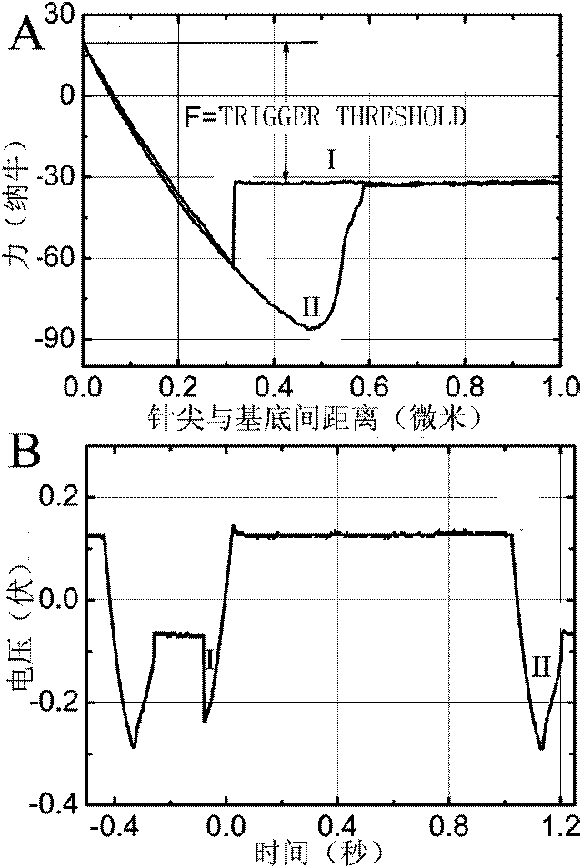
[0024] Etching is carried out in an environment with a relative humidity of 78% to 85% using an NSC-18 needle tip. The force used was 20nN, the sample was a silicon wafer treated with hexamethoxydisilane, and the ink was glycerol. Adjust TRIGGER TRESHOLD until figure 2 A force curve in the shape of A appears. If a force curve with a complete shape cannot be obtained, no matter how long the contact time is, the etching cannot be successful. figure 2 In B, it can be seen that the SURFACE DELAY time between point 3 and point 4 is 1s.
Embodiment 2
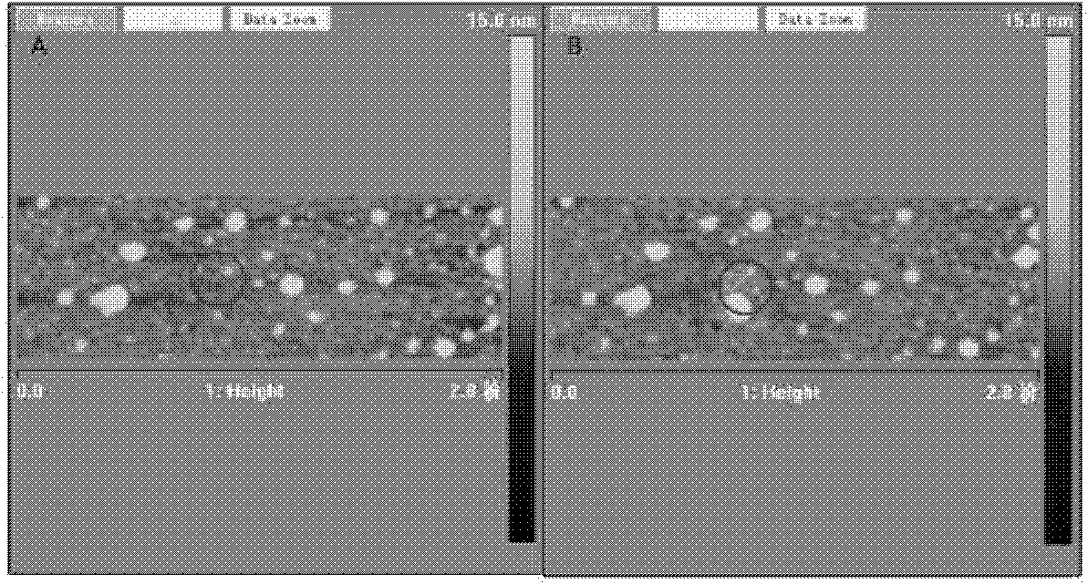
[0026] Etching is carried out in an environment with a relative humidity of 78% to 85% using an NSC-18 needle tip. The force used is 20nN, the sample is a silicon wafer after silane hydrophobic treatment, and the ink is glycerin. Points obtained by precisely controlling the residence time of the needle tip on the sample surface for 10 seconds. image 3 A is the pattern on the surface of the silicon wafer before etching, image 3 B is the pattern after etching. Comparing the two figures, it can be seen that under this condition, the method can successfully realize the etching of nano-dots.
Embodiment 3
[0028] Etching is carried out in an environment with a relative humidity of 43.4% to 46.5% using NSC-11 needle tips. Figure 4 A: The force used is 40nN, the sample is newly dissociated mica, the ink is glycerol, the residence time of the needle tip on the sample surface is precisely controlled to 20 seconds, and a nano-pattern with an interval of 400nm is obtained. Figure 4 B is the force used is 80nN, the sample is newly dissociated mica, the ink is horseradish peroxidase, and the residence time is 30 seconds, the obtained "口"-shaped nano-lattice array. Comparing the two figures, it can be seen that the nanodot array can be successfully obtained by this method; and because the force and time are well controlled, the shape and size of these dots are very consistent under the same operating parameters.
PUM
 Abstract
Description
Claims
Application Information
 - R&D
- Intellectual Property
- Life Sciences
- Materials
- Tech Scout
- Unparalleled Data Quality
- Higher Quality Content
- 60% Fewer Hallucinations
Browse by: Latest US Patents, China's latest patents, Technical Efficacy Thesaurus, Application Domain, Technology Topic, Popular Technical Reports.
© 2025 PatSnap. All rights reserved.Legal|Privacy policy|Modern Slavery Act Transparency Statement|Sitemap|About US| Contact US: help@patsnap.com


