
Process for cutting silicon chip by using steel wire with diameter of 0.11 millimeter

A cutting process and steel wire technology, which is used in the process of cutting silicon wafers with a steel wire with a diameter of 0.11mm, to achieve the effect of reducing cutting loss, reducing cutting loss and improving the quality of cutting surface

Inactive Publication Date: 2011-05-18
TIANJIN HUANOU SEMICON MATERIAL TECH CO LTD
View PDF5 Cites 24 Cited by
  • Summary
  • Abstract
  • Description
  • Claims
  • Application Information

AI Technical Summary

Problems solved by technology

[0003] The technical problem to be solved by the present invention is: on the premise of ensuring the quality of slices, provide a method to effectively improve the cutting rate per kilogram, reduce cutting consumption, reduce Production method of defective rate of cutting wire

Method used

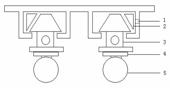
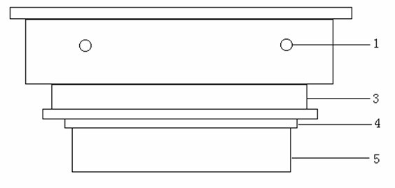
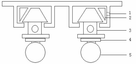

Image

  • Process for cutting silicon chip by using steel wire with diameter of 0.11 millimeter
  • Process for cutting silicon chip by using steel wire with diameter of 0.11 millimeter
  • Process for cutting silicon chip by using steel wire with diameter of 0.11 millimeter

Examples


Embodiment Construction

[0018] Specific examples are given below to further illustrate how the present invention is realized.

[0019] 1. The main equipment and raw materials of this embodiment are as follows:

[0020] Multi-wire cutting machine model: 442D; raw material: zone-melted (CZ) silicon single crystal, the cutting specification of this example is 3 inches thick silicon wafers with a thickness of 300um, the following is the production method and details of using 0.11mm diameter steel wires for silicon wafer cutting Process:

[0021] (1) Mortar configuration: The operator will dry the corundum, the drying temperature is 40-70 degrees, and the drying time is 20-60 minutes. This example uses 40 minutes. Calculate the amount of cutting fluid and emery according to the ratio (in this example, the mass ratio is cutting fluid: emery = 1:0.9), weigh them, and prepare the mortar in the mixing tank. The mixing time is 6-24 hours. This example uses 12 Hour.

[0022] (2) Orientation and stick...


PUM


Abstract

The invention relates to a process for cutting a silicon chip by using a steel wire with a diameter of 0.11 millimeter. On a multi-wire cutter, the steel wire with the diameter of 0.11 millimeter, cutting fluid and carborundum are used as main auxiliary materials for cutting and processing the silicon chip. The process comprises the steps of mortar preparation, orientation, bar sticking, cutting preheating, cutting, blanking, degumming and cleaning. The steel wire with the diameter of 0.11 millimeter and with proper tension and cutting speed is matched with the cutting fluid and the carborundum to obtain a better cutting surface and effectively reduce the cutting loss; compared with the universally adopted steel wires with diameters of 0.14 millimeter and 0.12 millimeter, the steel wire with the diameter of 0.11 millimeter can save the raw materials by 6.45 percent and 2.15 percent; and the thinner the silicon chip is, the more obvious the benefit is.

Description

technical field [0001] The invention relates to a process for slicing semiconductor silicon wafers, in particular to a process for cutting silicon wafers with a steel wire with a diameter of 0.11 mm. Background technique [0002] As we all know, the basis of modern information technology and modern electronic technology is semiconductor technology, and semiconductor silicon single crystal material is the most important semiconductor material. The biggest cost in semiconductor material processing is the cost of raw materials, which accounts for more than 50% of the silicon wafer processing cost. Multi-wire cutting machines are widely used in the field of cutting large-diameter ultra-thin silicon wafers with extremely high production efficiency and wafer yield. By improving the diameter of the steel wire and adjusting the process, the number of pieces processed and the yield of the product can be increased. Contents of the invention [0003] The technical problem to be s...

Claims


Application Information

Patent Timeline
IPC IPC(8): B28D5/04
Inventor 刘涛靳立辉郭红慧范猛孙红永张雪囡李翔沈浩平
Owner TIANJIN HUANOU SEMICON MATERIAL TECH CO LTD
Learn More