Manufacturing method of laterally diffused metal oxide semiconductor element

A technology of oxide semiconductor and manufacturing method, which is applied in semiconductor/solid-state device manufacturing, electrical components, circuits, etc., and can solve problems such as misalignment, relative position error, affecting channel length

Inactive Publication Date: 2011-05-04
UNITED MICROELECTRONICS CORP
View PDF0 Cites 0 Cited by
  • Summary
  • Abstract
  • Description
  • Claims
  • Application Information

AI Technical Summary

Problems solved by technology

However, in the known method for fabricating laterally diffused metal oxide semiconductor devices, when a photomask defining a P-type doped region is used for photolithography, the pattern of the photomask of the P-type doped region is different from that defined in the previous layer. The photomask pattern of the source element region is aligned, and when the photolithography process is performed using the photomask forming the gate structure, the photomask pattern of the gate structure is also aligned with the photomask pattern of the active element region of the previous layer Alignment, which makes the position of the photomask pattern of the P-type doped region and the position of the photomask pattern of the gate structure an indirect alignment relationship, so the relative position of the two is prone to errors, resulting in the P-type doped region and the gate structure. The relative position of the gate structure produces misalignment, which in turn affects the size of the channel length

Method used


Image

  • Manufacturing method of laterally diffused metal oxide semiconductor element
  • Manufacturing method of laterally diffused metal oxide semiconductor element
  • Manufacturing method of laterally diffused metal oxide semiconductor element

Examples


no. 1 example

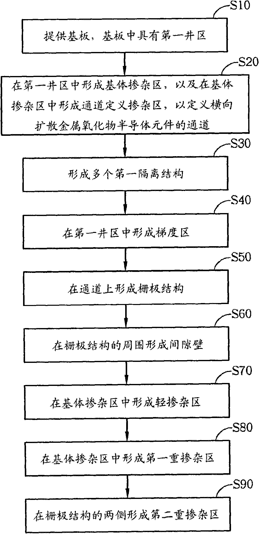
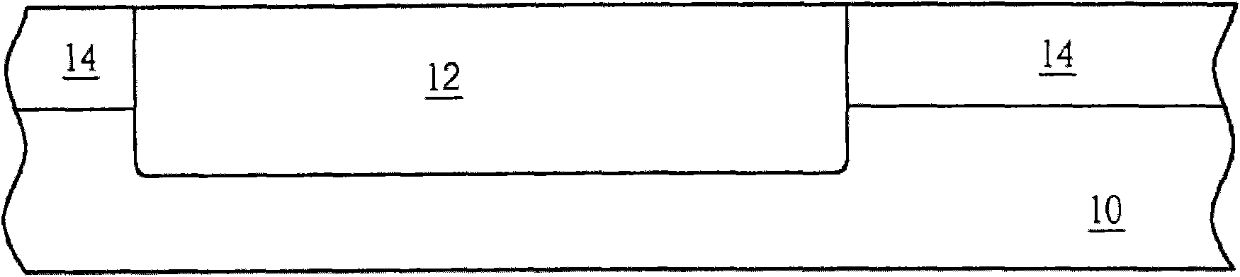
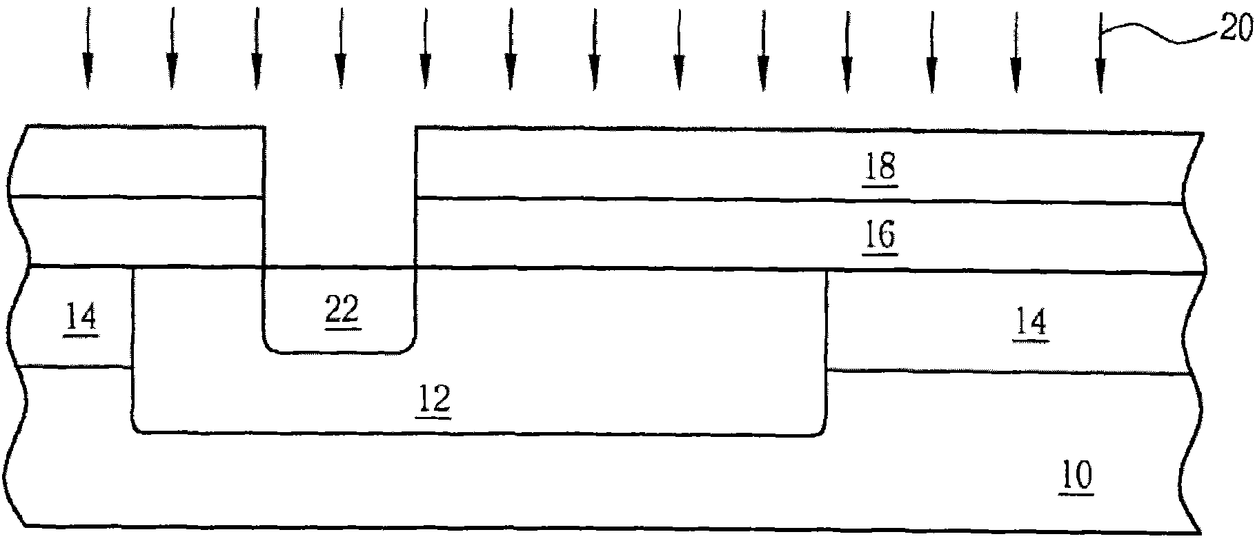
[0053] Additionally, please refer to Figure 12 and Figure 13 , Figure 12 It is a schematic flow chart of the manufacturing method of the laterally diffused semiconductor element according to the second embodiment of the present invention, Figure 13 It is a schematic diagram of the manufacturing method of the laterally diffused semiconductor device according to the second embodiment of the present invention. Compared with the first embodiment, the manufacturing method of the second embodiment is used for manufacturing a laterally diffused semiconductor device whose gate structure and drain end can withstand high breakdown voltage. The method of this embodiment before step S20 and after step S50 is the same as that of the first embodiment. In order to facilitate the comparison of the differences between the embodiments, the same steps of this embodiment and the first embodiment will not be repeated, and the same components Symbols are marked with the same symbols. Such a...


PUM


Abstract

The invention discloses a manufacturing method of a laterally diffused metal oxide semiconductor element. The manufacturing method is as follows: a providing a substrate with a first conduction type, wherein the substrate is internally provided with a well area with a second conduction type; then, forming a substrate doping area in the well area and forming a channel definition doping area in the substrate doping area, wherein the substrate doping area is provided with the first conduction type, and the channel definition doping area is provided with the second conduction type; utilizing the substrate doping area which is positioned between the channel definition doping area and the well area and is not covered by the channel definition doping area to form a channel of the laterally diffused metal oxide semiconductor element; and then, forming a grid structure on the channel. Therefore, by utilizing the manufacturing method, the channel change due to displacement of the grid structure can be avoided.

Description

technical field [0001] The invention relates to a method for manufacturing a lateral-diffusion metal-oxide-semiconductor (LDMOS) element, in particular to a method for manufacturing a lateral-diffusion metal-oxide-semiconductor element with a stable channel length. Background technique [0002] Metal-oxide-semiconductor devices are electronic devices often used in integrated circuits. A metal oxide semiconductor element is a semiconductor element composed of different electrodes such as a gate, a source, and a drain. It is mainly used for gate-to-gate The voltage induces charges between the source and the drain to form a channel, which makes the source and the drain conduct. Therefore, it can be used as a digitalized solid-state switch to be used in various applications with other components. IC products for logic and memory. [0003] It is known that the laterally diffused metal oxide semiconductor device includes a P-type base doped region and a gate structure, and its c...

Claims


Application Information

Patent Timeline
IPC IPC(8): H01L21/336H01L21/265
Inventor 黄柏睿
Owner UNITED MICROELECTRONICS CORP
Why Eureka
Try Eureka