Embedded resistor structure and manufacturing method thereof

A manufacturing method and technology of embedding resistors, which are applied in directions including printed resistors, printed circuit manufacturing, and removal of conductive materials by chemical/electrolytic methods. It can solve the problems of multiple resistor manufacturing processes and difficult control of resistor wires, and achieve line protection. The effect of no change and less process

Inactive Publication Date: 2020-06-05
QING DING PRECISION ELECTRONICS HUAIAN CO LTD +1
View PDF7 Cites 0 Cited by
  • Summary
  • Abstract
  • Description
  • Claims
  • Application Information

AI Technical Summary

Problems solved by technology

This method requires multiple etchings, resulting in more manufacturing processes for resistors, and it is difficult to control the shape of resistors.

Method used


Image

  • Embedded resistor structure and manufacturing method thereof
  • Embedded resistor structure and manufacturing method thereof
  • Embedded resistor structure and manufacturing method thereof

Examples


Embodiment Construction

[0030] In order to further illustrate the technical means and effects that the present invention takes to reach the intended purpose of the invention, the following in conjunction with the appended Figure 1-9 And the preferred implementation mode, the specific implementation mode, structure, characteristics, method and effect of the embedded resistor and its manufacturing method provided by the present invention are described in detail as follows.

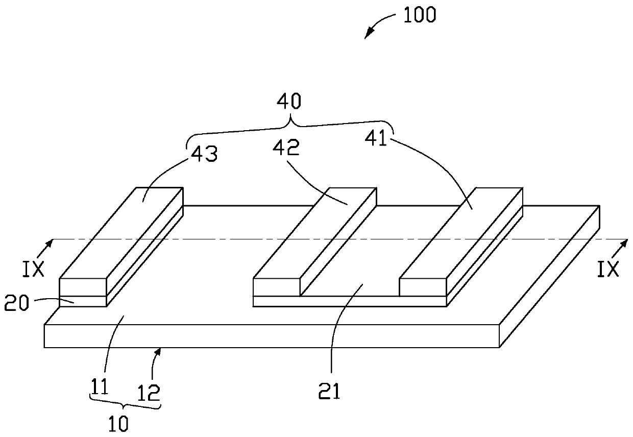
[0031] see figure 1 , the present invention provides a buried resistor structure 100 .

[0032] Wherein, the embedded resistor structure 100 may be a single-sided embedded resistor, or may be a double-sided embedded resistor. In this embodiment, the embedded resistor structure 100 is a single-sided embedded resistor.

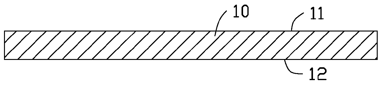
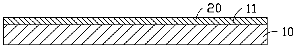
[0033] Specifically, the embedded resistance structure 100 includes a substrate layer 10 , a resistance material layer 20 and a copper plating layer 40 . Wherein, the resistive material layer 20 is formed on the ...


PUM


Abstract

The invention discloses a manufacturing method of an embedded resistor structure. The method comprises the following steps of: providing a substrate layer, forming a resistance material layer on the base material layer in a chemical plating mode, forming a copper plating layer on the surface, away from the base material layer, of the resistance material layer to obtain an embedded resistance structure intermediate, the copper plating layer comprising a first conductive circuit and a second conductive circuit, and the resistance material layer being exposed between the first conductive circuitand the second conductive circuit, forming an anti-plating film layer on the copper plating layer, the anti-plating film layer covering the resistance material layer between the first conductive circuit and the second conductive circuit, and etching off the uncovered resistance material layer through a chemical reagent, and removing the anti-plating film layer. The invention also relates to an embedded resistor structure.

Description

technical field [0001] The invention relates to a printed circuit board technology, in particular to an embedded resistance structure and a manufacturing method thereof. Background technique [0002] With the development of electronic products in the direction of lightness, thinness, shortness, smallness, multi-function, modularization, and integration, printed circuit boards (PCBs) as mounting components also require finer and denser circuits, and also require energy To reserve more mounting space for active chips, embedded passive device technology emerges as the times require, such as embedded capacitors, embedded resistors, and embedded inductance technologies, which have gradually become an inevitable trend in the development of PCBs. [0003] Embedded resistor technology is a kind of embedded passive device technology, which means that the traditional resistors that need to be installed on the surface of the PCB are all or partially buried inside the PCB, which reserve...

Claims


Application Information

Patent Timeline
IPC IPC(8): H05K1/16H05K3/06
CPCH05K1/167H05K3/06H05K3/061H05K2203/1377
Inventor 胡先钦沈芾云何明展徐筱婷
Owner QING DING PRECISION ELECTRONICS HUAIAN CO LTD
Why Eureka
Try Eureka