Method for preparing stress-free GaN thick film on sapphire patterned substrate

A graphics substrate, sapphire technology, applied in semiconductor/solid-state device manufacturing, electrical components, circuits, etc., can solve problems such as substrate pollution and easy cracking

Inactive Publication Date: 2011-04-27
INST OF SEMICONDUCTORS - CHINESE ACAD OF SCI
View PDF0 Cites 8 Cited by
  • Summary
  • Abstract
  • Description
  • Claims
  • Application Information

AI Technical Summary

Problems solved by technology

It overcomes the problem that the heteroepitaxial GaN thick film is easy to crack, and also avoids the problem of substrate contamination and damage

Method used


Image

  • Method for preparing stress-free GaN thick film on sapphire patterned substrate
  • Method for preparing stress-free GaN thick film on sapphire patterned substrate
  • Method for preparing stress-free GaN thick film on sapphire patterned substrate

Examples


Embodiment 1

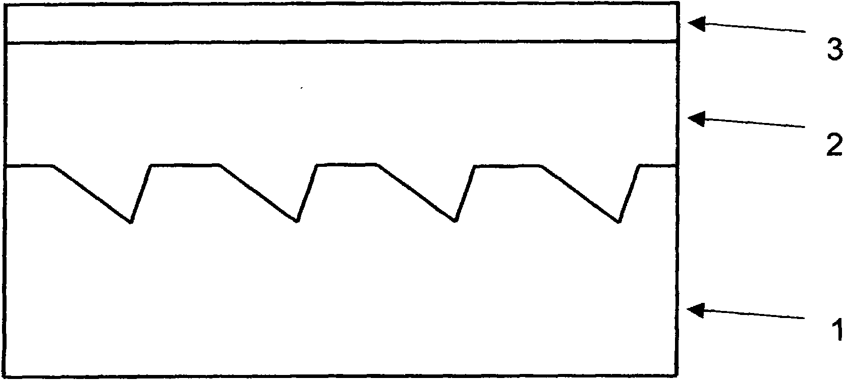
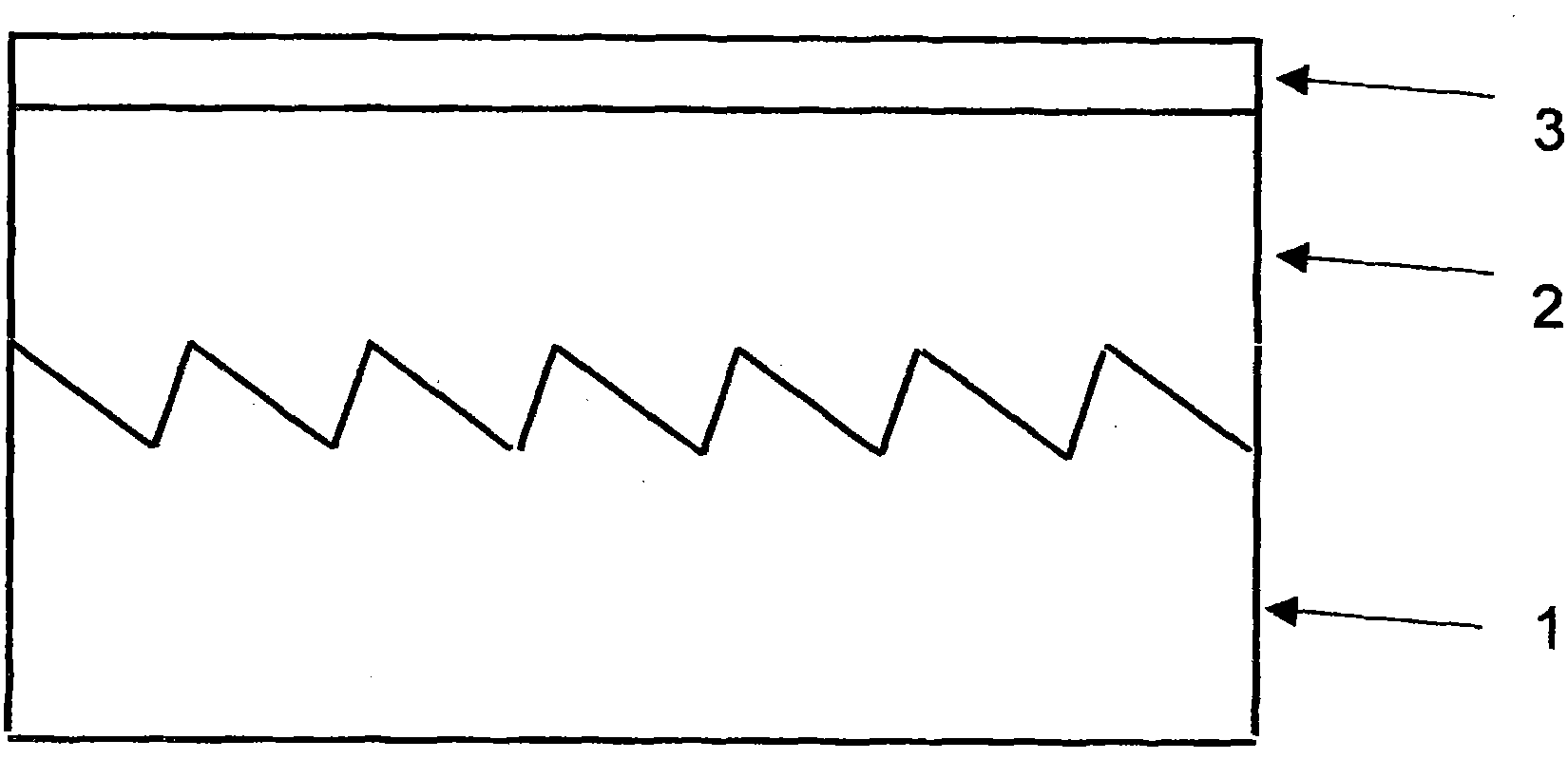
[0024] see figure 1 Shown, a kind of method of the present invention prepares stress-free GaN thick film on sapphire pattern substrate, comprises the following steps:

[0025] Step 1. Deposit a layer of silicon dioxide or silicon nitride film (not shown) on the C-face sapphire substrate; wherein the thickness of the silicon dioxide or silicon nitride film is 10 nm to 5 μm; this example uses plasma Enhanced chemical vapor deposition technology evaporates a silicon dioxide film with a thickness of 300nm on the C-plane sapphire substrate.

[0026] Step 2, using conventional photolithography techniques to photoetch striped silicon dioxide or silicon nitride mask patterns along the [11-20] direction on the C-plane sapphire substrate deposited with silicon dioxide or silicon nitride; Wherein the strip-shaped silicon dioxide or silicon nitride mask pattern is along the [11-20] direction, the strip-shaped silicon dioxide or silicon nitride mask pattern is striped, and its width is 1 ...

Embodiment 2

[0032] see figure 2 , present embodiment 2 is basically the same as embodiment 1, and its difference is:

[0033](1) In step 2, standard photolithography process is used to photoetch the strip-shaped silicon dioxide mask pattern along the [11-20] direction on the sapphire substrate. The photolithography process includes glue coating, exposure and etching. Standard processes such as silicon oxide and glue removal, the width of the prepared silicon dioxide mask layer stripes is 2 μm, and the width of the window area is 5 μm.

[0034] (2) After step 3 was completed, a clean sapphire pattern substrate 1 different from Example 1 was obtained. It can be seen that the corroded grooves are V-shaped, and the V-shaped grooves are regularly arranged on the substrate. Each The period is 7 μm. There is no platform between the V-shaped grooves, and the sapphire pattern substrate 1 is zigzag. The depth of the V-shaped groove is 3 μm, and the two sides are asymmetrical, the short side cor...


PUM

PropertyMeasurementUnit
Thicknessaaaaaaaaaa

Abstract

The invention relates to a method for preparing a stress-free GaN thick film on a sapphire patterned substrate, which comprises the following steps: 1, depositing a silicon oxide or silicon nitride film on a C-plane sapphire substrate; 2, photoetching bar-shaped silicon oxide or silicon nitride mask patterns in a [11-20] direction on the C-plane sapphire substrate of the deposited silicon oxide or silicon nitride film by the conventional photoetching technology; 3, transferring the photoetched bar-shaped silicon oxide or silicon nitride mask patterns onto the substrate by wet-process etching; 4, removing the silicon oxide or silicon nitride film by corrosion, and cleaning the substrate to obtain a clean sapphire patterned substrate; and 5, directly using a hydride gas-phase epitaxy system to epitaxially grow a GaN thick film on the obtained sapphire patterned substrate, and thus finishing the preparation.

Description

technical field [0001] The invention relates to a method for preparing a stress-free GaN thick film on a sapphire pattern substrate. Background technique [0002] GaN is the third-generation semiconductor material developed rapidly after the first-generation semiconductor material represented by silicon and the second-generation semiconductor material represented by gallium arsenide. GaN has a direct energy band structure with a bandgap width of 3.4eV. It also has the characteristics of high thermal conductivity, high electron saturation drift rate, high breakdown field strength, and small dielectric constant. Therefore, it has broad application prospects in many fields such as blue, green and ultraviolet light-emitting diodes (LEDs), short-wavelength laser diodes (LDs), ultraviolet detectors, and power electronic devices. [0003] Since the preparation of GaN bulk single crystal is difficult, and it is difficult to obtain a bulk single crystal GaN substrate with a large si...

Claims


Application Information

Patent Timeline
IPC IPC(8): H01L21/205H01L21/311H01L21/306
Inventor 胡强段瑞飞魏同波杨建坤霍自强曾一平
Owner INST OF SEMICONDUCTORS - CHINESE ACAD OF SCI
Why Eureka
Try Eureka