Solid-state image pickup apparatus and X-ray inspection system

A solid-state imaging device and X-ray technology, which is applied in the direction of electric solid-state devices, radiation control devices, TV system components, etc., can solve the problem that the solid-state imaging device cannot perform high-speed actions

Active Publication Date: 2013-05-15
HAMAMATSU PHOTONICS KK
View PDF1 Cites 1 Cited by
  • Summary
  • Abstract
  • Description
  • Claims
  • Application Information

AI Technical Summary

Problems solved by technology

However, the present inventors have found that there is a problem to be solved that the solid-state imaging device cannot perform high-speed operation due to the configuration of the solid-state imaging device.

Method used


Image

  • Solid-state image pickup apparatus and X-ray inspection system
  • Solid-state image pickup apparatus and X-ray inspection system
  • Solid-state image pickup apparatus and X-ray inspection system

Examples


Embodiment Construction

[0030] Hereinafter, the best mode for carrying out the present invention will be described in detail with reference to the drawings. In addition, in the description of the drawings, the same reference numerals are given to the same elements, but overlapping descriptions are omitted.

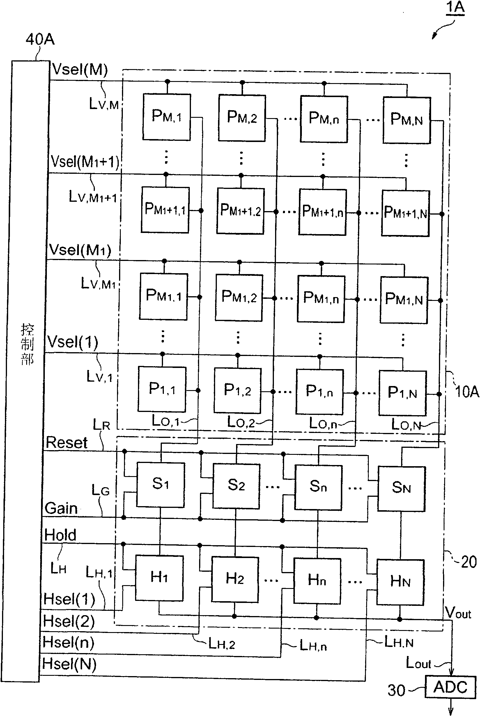
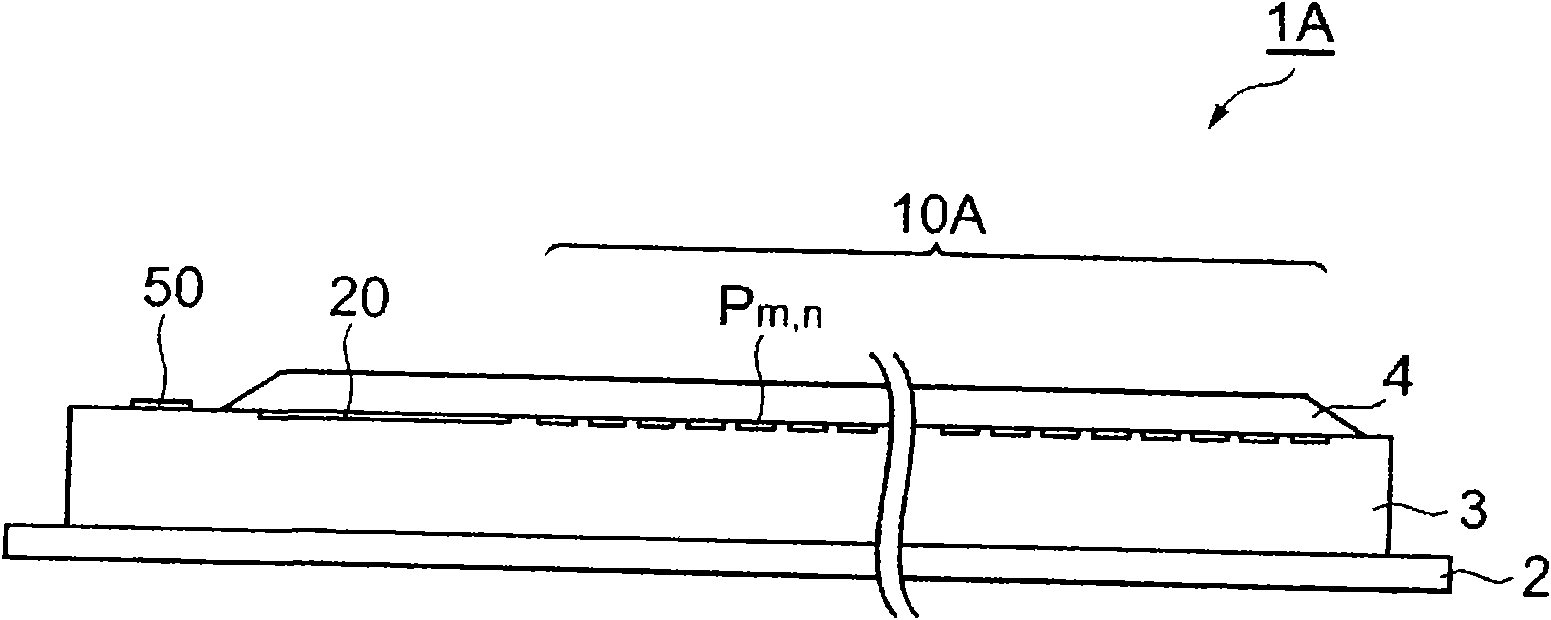
[0031] First, the solid-state imaging device 1A according to the first embodiment will be described. figure 1 A diagram showing the configuration of a solid-state imaging device 1A according to the first embodiment. The solid-state imaging device 1A shown in this figure includes a light receiving unit 10A, a signal readout unit 20 , an A / D conversion unit 30 , and a control unit 40A. In addition, when used for X-ray detection, a scintillator unit is provided so as to cover the light receiving unit 10A of the solid-state imaging device 1A.

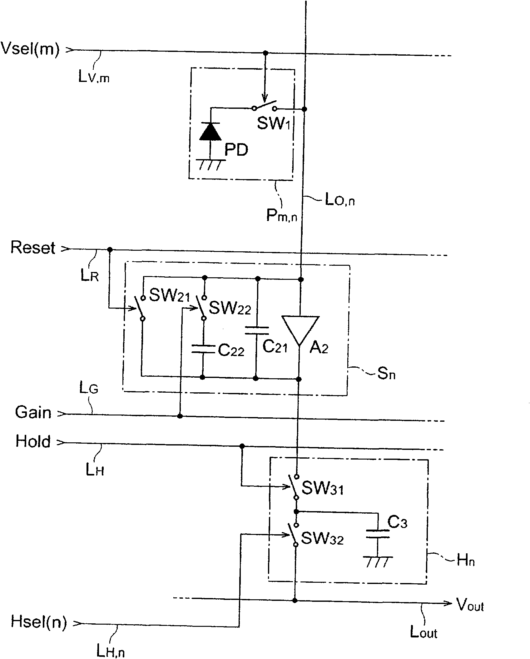
[0032] The light receiving unit 10A is M×N pixel units P 1,1 ~P M,N The 2-dimensional arrangement is M rows and N columns. Pixel part P m,n Located at r...


PUM


Abstract

A solid-state image pickup apparatus 1A includes a photodetecting section 10A, a signal readout section 20, and a controlling section 40A. In the photodetecting section 10A, M×N pixel units P 1,1 to P M,N each including a photodiode and a readout switch are arrayed in M rows and N columns. Charges generated in each pixel unit P m,n are input to an integrating circuit S n through a readout wiring L O,n , and a voltage value output from the integrating circuit S n in response to the charge amount is output through a holding circuits H n . When in a first imaging mode, a voltage value according to an amount of charges generated in the photodiode PD of each of the M×N pixel units P 1,1 to P M,N in the photodetecting section 10A is output from the signal readout section 20. When in a second imaging mode, a voltage value according to an amount of charges generated in the photodiode PD of each pixel unit P m,n included in consecutive M 1 rows in the photodetecting section 10A is output from the signal readout section 20.

Description

technical field [0001] The present invention relates to a solid-state imaging device and an X-ray inspection system. Background technique [0002] As a solid-state imaging device, it is generally known to use CMOS technology, and among them, a passive pixel sensor (PPS: Passive Pixel Sensor) system is generally known. The solid-state imaging device of the PPS method includes a light-receiving unit in which PPS-type pixel units are two-dimensionally arranged in M ​​rows and N columns. In each pixel unit, charges generated in photodiodes corresponding to incident light are stored in an integrating circuit. The capacitor outputs a voltage value corresponding to the amount of stored charge, and the PPS-type pixel unit includes a photodiode that generates an amount of charge corresponding to the intensity of incident light. [0003] In general, each output terminal of each of the M pixel units in each column is connected to an input terminal of an integrating circuit provided co...

Claims


Application Information

Patent Timeline
Patent Type & Authority Patents(China)
IPC IPC(8): H04N5/32H04N5/353H04N5/3745A61B6/03A61B6/00H01L27/14H01L27/146H04N5/335H04N5/369H04N5/374
CPCH04N5/3745H04N5/23245H01L27/14609A61B6/032H04N5/3454H04N5/32H04N5/343H04N23/667H04N25/42H04N25/443H04N25/77
Inventor 久嶋龙次藤田一树森治通
Owner HAMAMATSU PHOTONICS KK
Why Eureka
Try Eureka