
Method for manufacturing light-emitting diode (LED) structure

A technology of light-emitting diodes and diodes, applied in electrical components, circuits, semiconductor devices, etc., can solve problems such as emission wavelength drift, chip temperature rise, and affect chip luminous efficiency, and achieve the effect of improving lumen efficiency

Inactive Publication Date: 2011-02-02
JIANGXI HUAYE ENERGY SAVING LIGHTING
View PDF0 Cites 3 Cited by
  • Summary
  • Abstract
  • Description
  • Claims
  • Application Information

AI Technical Summary

Problems solved by technology

For this method of realizing white light, most of them mix yellow phosphor powder and epoxy resin evenly and coat it directly on the chip. Due to the light conversion in the yellow phosphor powder coating, the energy loss during the conversion process from blue light to yellow light Converted into heat, therefore, the temperature of the yellow phosphor coating is relatively high, and the temperature of the chip also increases accordingly, thus affecting the luminous efficiency of the chip
At the same time, the increase in temperature causes the emission wavelength to drift, which affects the light color. In addition, due to the close contact between the phosphor and the chip, the light emitted by the LED chip and the light emitted by the chip exciting the yellow phosphor are scattered back to the chip and absorbed by the chip. loss, leading to a decrease in light extraction efficiency

Method used


Image

  • Method for manufacturing light-emitting diode (LED) structure
  • Method for manufacturing light-emitting diode (LED) structure
  • Method for manufacturing light-emitting diode (LED) structure

Examples


Embodiment Construction

[0026] The method for manufacturing the light emitting diode structure of the present invention will be further described in detail below with reference to the accompanying drawings.

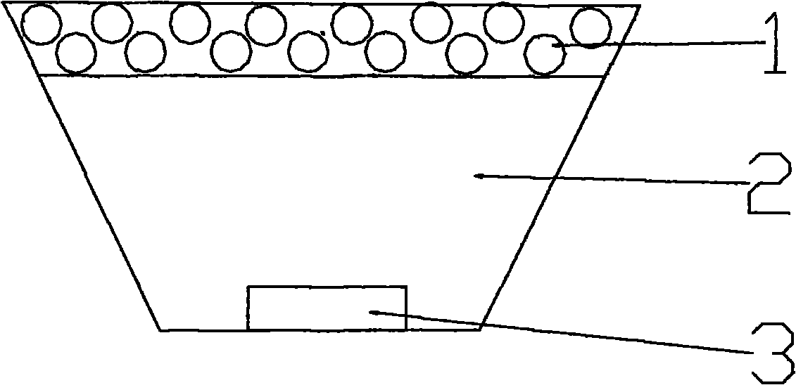
[0027] Such as figure 1 As shown, the present invention is a method for manufacturing a method for manufacturing a light-emitting diode structure, characterized in that the method for manufacturing a method for manufacturing a light-emitting diode structure includes the following steps:

[0028] 1) The cured and packaged blue light emitting diode chip and the corresponding lead structure are prepared, and the blue light emitting diode chip is electrically connected and fixed to the wires in the lead structure;

[0029] 2) Apply transparent epoxy resin on the blue light-emitting diode chip that has been cured, packaged and electrically connected to the lead structure. The epoxy resin does not contain phosphor powder, and then cured. Thin, the thinner the coating thickness, the better the LED lum...


PUM


Abstract

The invention discloses a method for manufacturing a light-emitting diode (LED) structure. The method comprises the following steps of: 1) preparing a cured and encapsulated blue LED chip and a corresponding lead wire structure, wherein the blue LED chip is electrically connected and fixed with the lead wire of the lead wire structure; 2) coating transparent epoxy resin on the blue LED chip which is fixed and connected with the lead wire structure and then performing curing, wherein the epoxy resin does not comprise fluorescent powder; 3) mixing yellow fluorescent powder and the epoxy resin uniformly and coating the yellow fluorescent powder and the epoxy resin which are mixed uniformly on the cured epoxy resin in the step 2) to perform secondary curing; and 4) performing encapsulation by using the epoxy resin. The method for manufacturing the LED structure has the advantages of effectively improving the luminous efficiency of a white LED and homogenizing the emitted light.

Description

technical field [0001] The invention relates to a method of manufacturing a light emitting diode structure. Background technique [0002] In recent years, the semiconductor light source that has been used for a long time in the display field, that is, Light Emitting Diode (Light Emitting Diode), LED is the abbreviation of Light Emitting Diode in English, and is gradually entering the lighting field as a new type of solid light source. Compared with traditional light sources, semiconductor light sources have the advantages of energy saving, high efficiency, small size, long life, fast response, low driving voltage, and anti-vibration. With the continuous reduction of its price and the continuous improvement of luminous brightness, semiconductor light sources have shown broad prospects in the field of lighting. [0003] The core of semiconductor lighting is to use semiconductor light-emitting technology to achieve white light. There are two main technical approaches to reali...

Claims


Application Information

Patent Timeline
Patent Type & Authority Applications(China)
IPC IPC(8): H01L33/00
Inventor 余建平陈太喜张玉生
Owner JIANGXI HUAYE ENERGY SAVING LIGHTING
Learn More