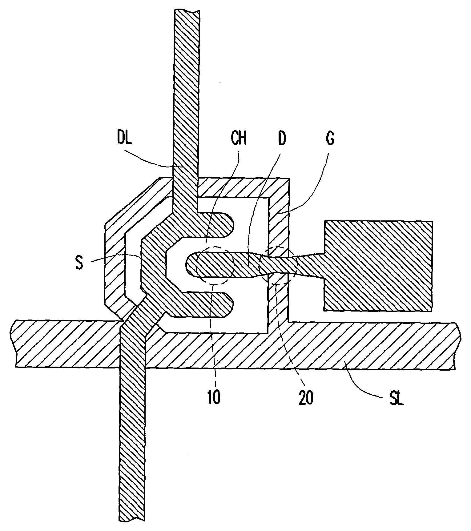
Thin film transistor, production method thereof and pixel structure
A thin-film transistor and pixel structure technology, which is applied in the direction of transistors, semiconductor/solid-state device manufacturing, electric solid-state devices, etc., can solve problems such as disconnection, component interference, and different drain D line widths.
- Summary
- Abstract
- Description
- Claims
- Application Information
AI Technical Summary
Problems solved by technology
Method used
Image
Examples
no. 1 example
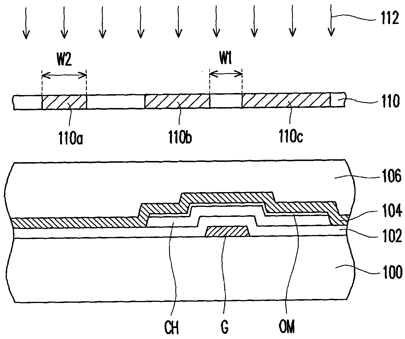
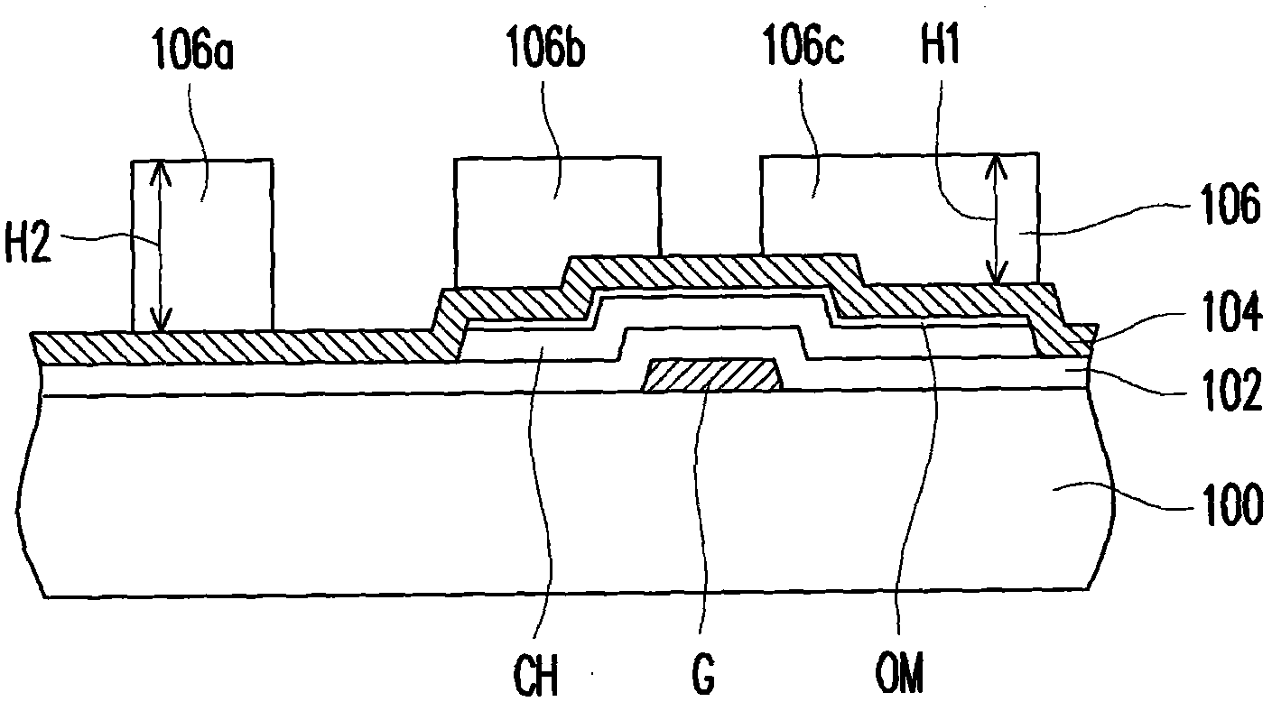
[0063] Figure 2A to Figure 2C is a schematic cross-sectional view of a manufacturing process of a thin film transistor according to an embodiment of the present invention. Please refer to Figure 2A , The manufacturing method of the thin film transistor of the present embodiment firstly includes providing a substrate 100 on which a gate G, an insulating layer 102 and a channel layer CH have been formed. According to a preferred embodiment, an ohmic contact layer OM is further formed on the channel layer CH.
[0064] The material of the substrate 100 can be glass, quartz, organic polymer, or opaque / reflective material (eg, conductive material, wafer, ceramic, or other applicable materials), or other applicable materials.
[0065] The gate G is formed on the substrate 100 . A method for forming the gate G is, for example, depositing a layer of conductive material on the substrate 100 first, and then patterning the conductive material to form the gate G through lithography an...
no. 2 example
[0077] Figure 4 is a schematic top view of a pixel structure according to an embodiment of the present invention. Figure 5 Yes Figure 4 The enlarged schematic diagram at 300 of . Please refer to Figure 4 as well as Figure 5 The pixel structure of this embodiment includes a data line DL, a first scan line SL1, a second scan line SL2, a first thin film transistor T1, a second thin film transistor T2, a third thin film transistor T3, a main pixel electrode PE1 and a sub pixel electrode PE2.
[0078] The first scanning line SL1 and the second scanning line SL2 are arranged in parallel, the first and second scanning lines SL1, SL2 and the data line DL are arranged alternately, and there is an insulating layer between the first and second SL1, SL2 and the data line DL. Floor. In other words, the extending direction of the data line DL is not parallel to the extending direction of the first and second scanning lines SL1 and SL2. Preferably, the extending direction of the d...
PUM
 Abstract
Description
Claims
Application Information
 - R&D Engineer
- R&D Manager
- IP Professional
- Industry Leading Data Capabilities
- Powerful AI technology
- Patent DNA Extraction
Browse by: Latest US Patents, China's latest patents, Technical Efficacy Thesaurus, Application Domain, Technology Topic, Popular Technical Reports.
© 2024 PatSnap. All rights reserved.Legal|Privacy policy|Modern Slavery Act Transparency Statement|Sitemap|About US| Contact US: help@patsnap.com


