Process of realizing p plus and n plus diffusion on both sides of silicon chip by utilizing mask
A silicon wafer surface and mask technology, applied in the field of solar cells, can solve the problems of cross-contamination of donor elements and acceptor elements, and achieve the effect of a practical diffusion process
- Summary
- Abstract
- Description
- Claims
- Application Information
AI Technical Summary
Problems solved by technology
Method used
Image

Examples
Embodiment 1
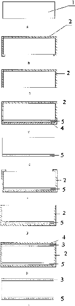
[0026] as attached figure 2 As shown, the implementation of p on both sides of the silicon wafer using a mask provided by this embodiment + and n + The diffusion process consists of the following steps:
[0027] (a) Select a p-type silicon wafer 1 with a resistivity of 0.1-10Ω·cm, and then clean the surface of the silicon wafer;
[0028] (b) prepare a layer of mask 2 on one side of the silicon wafer;
[0029] The mask is prepared by PECVD method, and the mask is SiOx thin film, which can also be prepared by sputtering, electron beam evaporation and other methods, and the mask can also be SiNx, SiCx, SiOxNy or SiCxNy thin film.
[0030] (c) Soak in HF solution, the volume percent content of HF solution is 5%, remove the mask around plating on the other side;
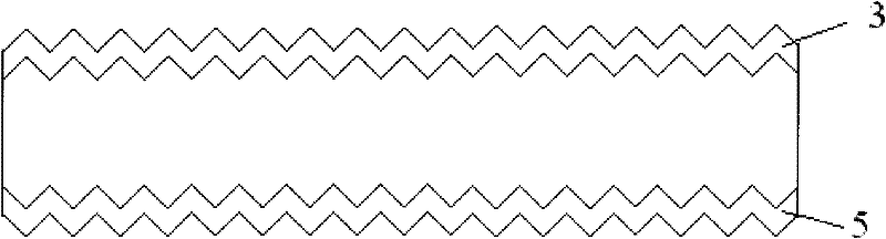
[0031] (d) Diffusion of the donor element phosphorus to form n on the unmasked side + Diffusion layer 5;
[0032] (e) soaking in 5% HF solution by volume to remove the doped glass 4 formed on the surface of the sil...
Embodiment 2
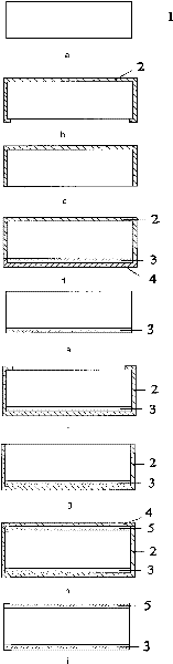
[0038] as attached image 3 As shown, the implementation of p on both sides of the silicon wafer using a mask provided by this embodiment + and n + The diffusion process consists of the following steps:
[0039] (a) select an n-type silicon wafer 1 with a resistivity of 0.1-10Ω·cm, and then clean the surface of the silicon wafer;
[0040] (b) prepare a layer of mask 2 on one side of the silicon wafer;
[0041] The mask can be prepared by spin-coating, spin-coating a layer of latex on the surface of the silicon wafer, and then drying to form a layer of SiO 2 mask.
[0042] (c) immerse in 5% HF solution by volume to remove the coating on the side without mask;
[0043] (d) Diffuse acceptor element boron to form p on the unmasked side + Diffusion layer 3;
[0044] (e) Soak in 5% HF solution by volume to remove the doped glass 4 formed in the mask and diffusion process;
[0045] (f) p on the silicon wafer + Surface preparation mask 2, the preparation method of the mask is...
Embodiment 3
[0050] This embodiment provides the use of masks to realize p on both sides of the silicon wafer. + and n + A diffusion process comprising the following steps:
[0051] (1) Select the silicon wafer after pretreatment such as cleaning, prepare a mask on one side of the silicon wafer, and remove the mask that is wrapped around the other side after it is made;
[0052] (2) Diffusion of donor elements or acceptor elements on the maskless side to form n + or p +Diffusion layer, and then remove the doped glass formed on the surface of the silicon wafer during the mask and diffusion;
[0053] (3) n formed in step (2) + or p + A mask is prepared on the surface of the diffusion layer, and the mask on the other side is removed after it is made;
[0054] (4) n made in step (3) + or p + The other side of the diffusion layer, that is, the side without a mask, undergoes diffusion of acceptor elements or donor elements to form p + or n + Diffusion layer, then cleaned to remove the ...
PUM
 Abstract
Description
Claims
Application Information
 - R&D
- Intellectual Property
- Life Sciences
- Materials
- Tech Scout
- Unparalleled Data Quality
- Higher Quality Content
- 60% Fewer Hallucinations
Browse by: Latest US Patents, China's latest patents, Technical Efficacy Thesaurus, Application Domain, Technology Topic, Popular Technical Reports.
© 2025 PatSnap. All rights reserved.Legal|Privacy policy|Modern Slavery Act Transparency Statement|Sitemap|About US| Contact US: help@patsnap.com