
Liquid crystal display device

A liquid crystal display device, liquid crystal technology, applied in nonlinear optics, instruments, optics, etc., can solve the problems of unstable liquid crystal molecular orientation, reduced transmittance, and uncomfortable pixels, etc., to achieve excellent contrast and viewing angle characteristics, The effect of improving brightness and high transmittance

Inactive Publication Date: 2010-12-22
SHARP KK
View PDF7 Cites 30 Cited by
  • Summary
  • Abstract
  • Description
  • Claims
  • Application Information

AI Technical Summary

Problems solved by technology

[0005] However, the above-mentioned MVA mode is not suitable for small pixels (for example, less than 100 μm on the short side, especially less than 60 μm)
Since the part where the slit (or rib) is installed does not contribute to the display, if it is applied to a pixel whose short side is less than 100 μm, the transmittance (brightness) will be extremely reduced
[0014] However, in the liquid crystal display device 90B, unlike the rivet 92 of the liquid crystal display device 90A, which exerts an alignment restricting force regardless of the presence of an electric field, since the alignment restricting force is only found when a voltage is applied, when the applied voltage is low, Orientation restriction force cannot be obtained sufficiently
Therefore, especially at a grayscale lower than the intermediate grayscale, there is a problem that the alignment of liquid crystal molecules is unstable, so it cannot be used practically.

Method used


Image

  • Liquid crystal display device
  • Liquid crystal display device
  • Liquid crystal display device

Examples


Embodiment Construction

[0059] Hereinafter, the configuration and operation of the liquid crystal display device according to the embodiment of the present invention will be described with reference to the drawings, but the present invention is not limited to the embodiment described below.

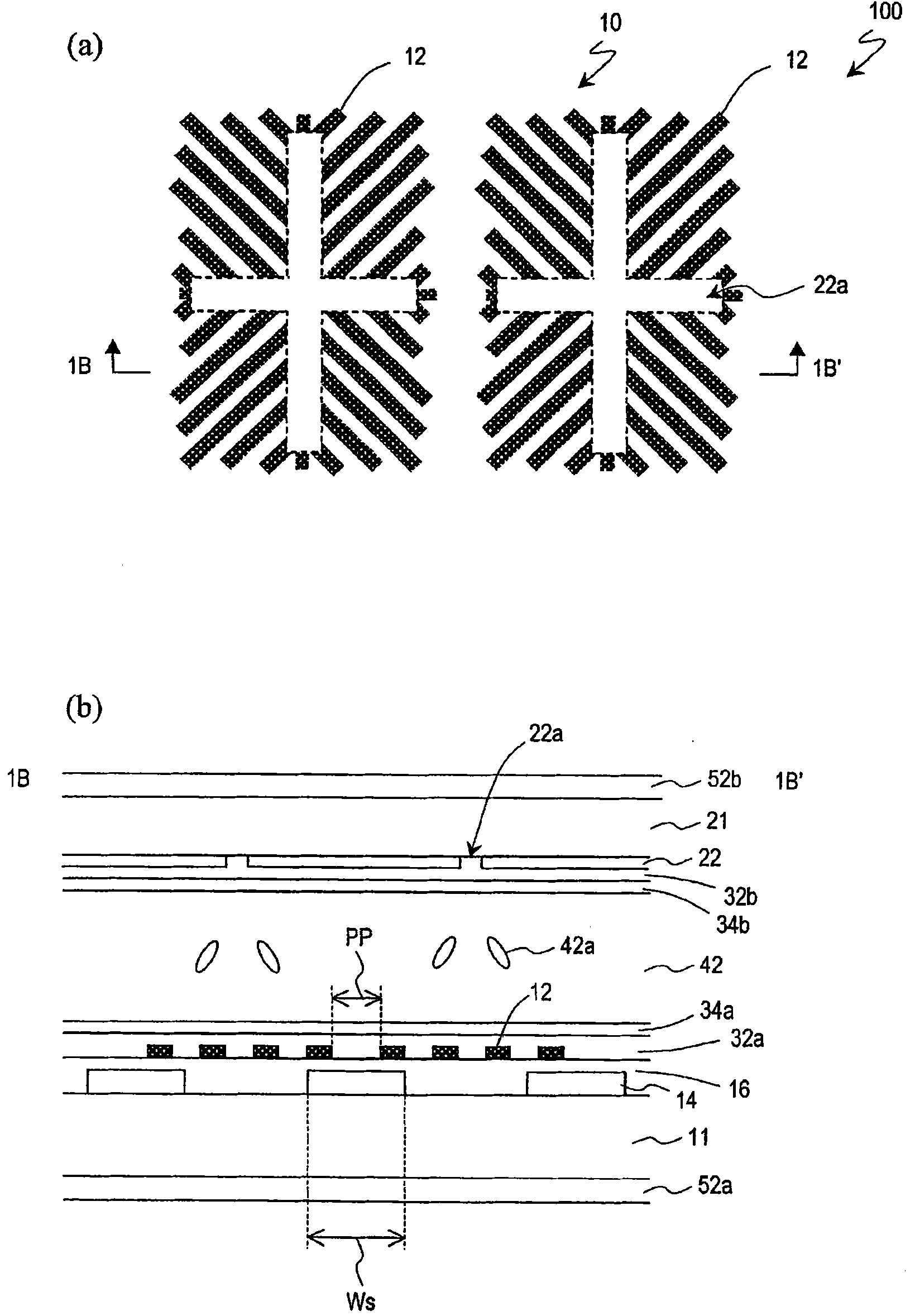
[0060] figure 1 Schematically showing the structure of two pixels 10 of the liquid crystal display device 100 according to the embodiment of the present invention, figure 1 (a) is a plan view, figure 1 (b) is along figure 1 (a) Cross-sectional view of line 1B-1B'.

[0061] The liquid crystal display device 100 is a liquid crystal display device that has a plurality of pixels, has a pair of substrates 11, 21 and a pair of polarizing plates 52b and 52b arranged outside them in a crossed Nicol configuration, and displays images in a normally black mode. . Each pixel has a liquid crystal layer 42 including a nematic liquid crystal material (liquid crystal molecules 42 a ) having a negative dielectric anisotr...


PUM

PropertyMeasurementUnit
particle diameteraaaaaaaaaa
thicknessaaaaaaaaaa

Abstract

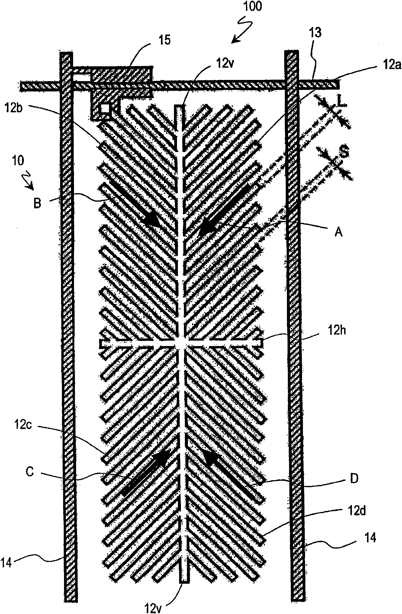
Provided is a liquid crystal display device having a pixel comprising a liquid crystal layer 42, a pixel electrode 12 and a counter electrode 22 confronting each other through the liquid crystal layer, a pair of vertically-oriented films 32a and 32b, and orientation maintaining layers 34a and 34b formed on the surfaces of the liquid crystal layer sides of the oriented films and made of a photochemically polymerized material. The pixel electrode includes cross-shaped trunks 12h and 12v arranged over the polarizing axes of a pair of polarizing plates, and a plurality of branches 12a, 12b, 12c and 12d extending in directions of about 45 degrees from the cross-shaped trunks. The counter electrode has a cross-shaped opening 22a arranged to confront the cross-shaped trunks. When a predetermined voltage is applied to the liquid crystal layer, four liquid crystal domains are formed, and the liquid crystal molecules of the regions corresponding individually to the four liquid crystal domains are specified in a pre-tilt azimuth by the orientation maintaining layers.

Description

technical field [0001] The present invention relates to a liquid crystal display device, and particularly relates to an alignment control structure suitably applied to a liquid crystal display device having a relatively small pixel pitch. Background technique [0002] Currently, as liquid crystal display devices having wide viewing angle characteristics, transverse electric field modes (including IPS mode and FFS mode) and vertical alignment (VA) modes are being used. Since the VA mode is superior to the transverse electric field mode in terms of mass productivity, it is widely used for TV applications and mobile applications. [0003] VA mode liquid crystal display devices are further broadly classified into MVA mode (see Patent Document 1) and CPA mode (see Patent Document 2). [0004] In the MVA mode, linear orientation-regulating units (slits or ribs) are arranged along two directions orthogonal to each other, and between the orientation-regulating units, the azimuth an...

Claims


Application Information

Patent Timeline
Patent Type & Authority Applications(China)
IPC IPC(8): G02F1/1343G02F1/1335G02F1/1337
CPCG02F1/134309G02F1/133707G02F1/1393
Inventor 桥本义人大上裕之柴崎正和久保真澄曾我雅之
Owner SHARP KK
Learn More