
Guide die structure for growing extra-thick monocrystal alumina wafer

A single-crystal alumina, extra-thick technology, applied in the directions of single-crystal growth, crystal growth, single-crystal growth, etc., can solve the problem of unsuitable growth of extra-thick large single-crystal alumina sheets, complex crystallizer core structure, and single crystal growth. Alumina sheet cracking and other problems, to achieve the effect of simple structure, high qualified rate of finished products and stable temperature field

Inactive Publication Date: 2010-12-01
无锡金岩光电晶体科技有限公司
View PDF5 Cites 7 Cited by
  • Summary
  • Abstract
  • Description
  • Claims
  • Application Information

AI Technical Summary

Problems solved by technology

However, because the crystallizer includes a mold core and a mold sleeve, the mold core is installed in the mold sleeve, and the mold core and the mold sleeve are processed from an integral molybdenum block with a large thickness. When growing single crystal alumina sheets, it is easy to cause temperature lag. Suitable for growing single crystal alumina ceramic tubes or 3mm ~ 5mm single crystal alumina ceramic tiles, not suitable for growing extra thick and large single crystal alumina tiles
At present, the thickness of a single-crystal aluminum oxide sheet used for growing a LED substrate by radio frequency in foreign countries is 5 mm, which requires subsequent cutting, grinding, and polishing processes after forming and growing, and the material utilization rate is low, and the final production cost is high; in addition, foreign countries In the crucible guide mode structure for growing and forming single crystal alumina flakes, after multi-mode is adopted to increase the feeding amount, the core structure of the crystallizer is complicated, and the temperature gradient at the growth crystallization table is large, which is easy to cause single crystal alumina Chip cracking, low yield of finished products

Method used


Image

  • Guide die structure for growing extra-thick monocrystal alumina wafer
  • Guide die structure for growing extra-thick monocrystal alumina wafer
  • Guide die structure for growing extra-thick monocrystal alumina wafer

Examples


Embodiment Construction

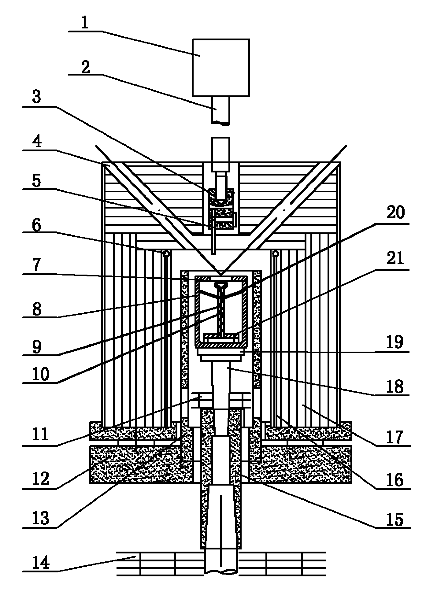
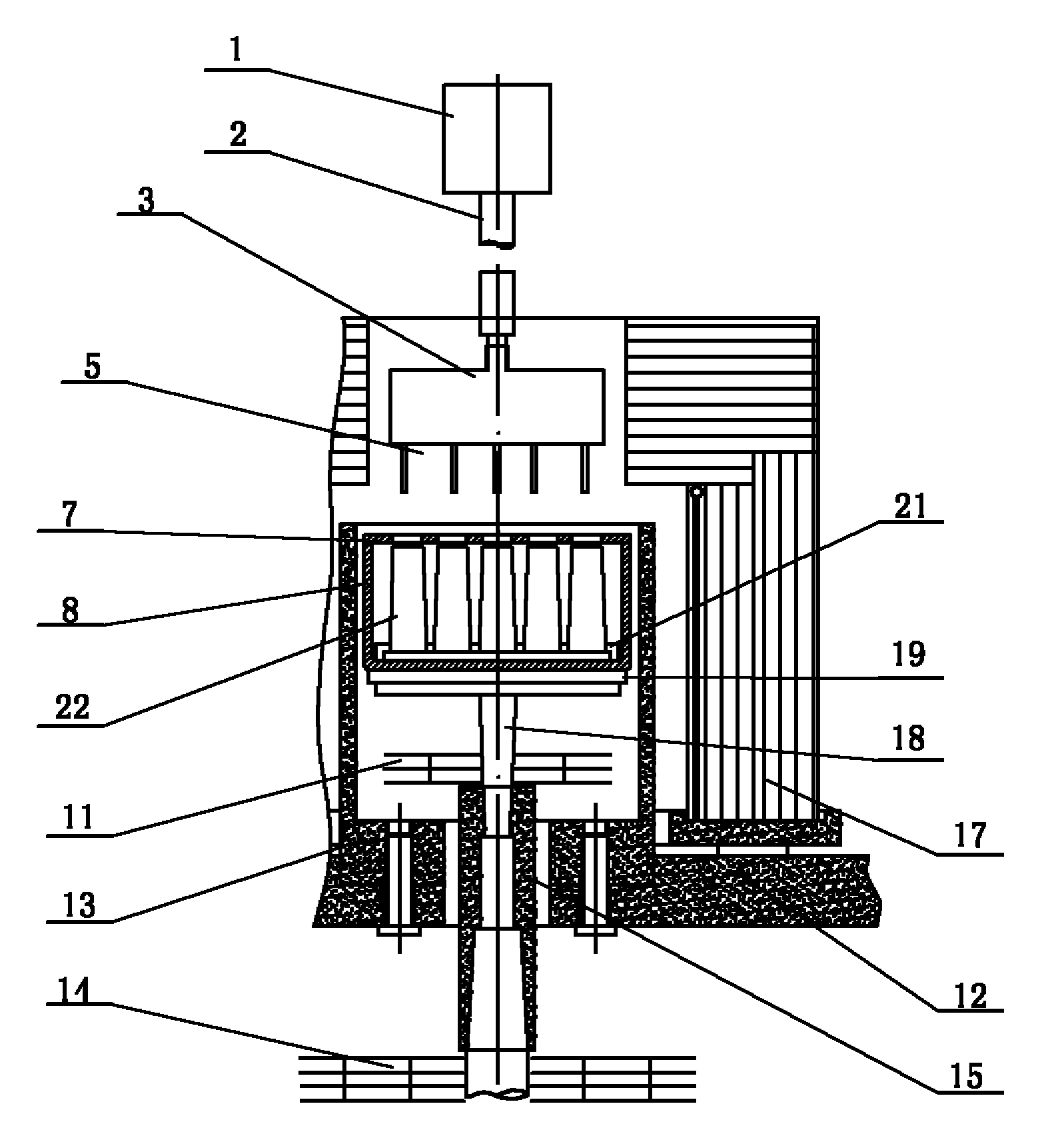
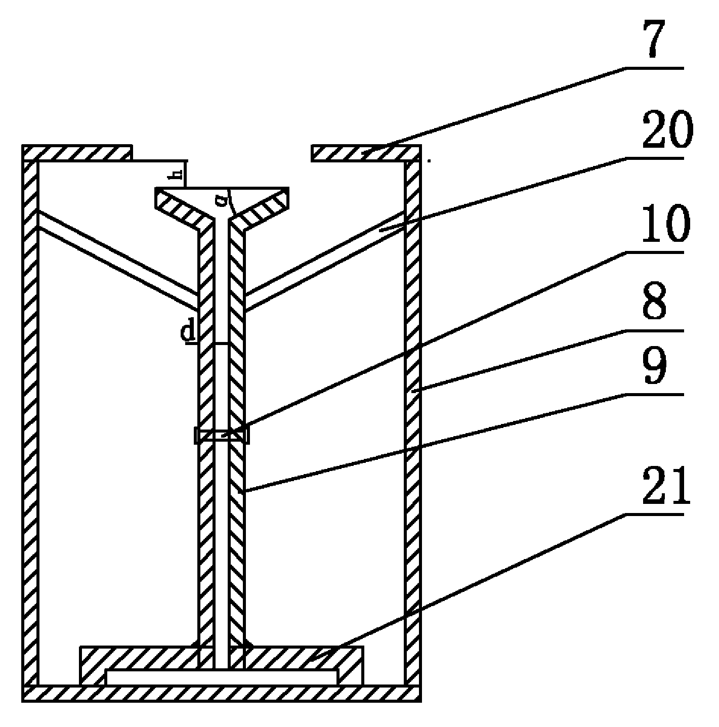
[0010] See figure 1 , figure 2 and image 3 , the present invention comprises crucible 8, and crucible 8 is installed in heater 13 by handle 18, and heater 13 is installed in electrode plate 12, and heater 13 is provided with insulation screen 17, and crucible 8 is provided with crystallizer 22, and crystallizer 22. A seed crystal 5 is arranged above the crystallization table, and the seed crystal 5 is connected to the seed crystal shaft sleeve 1 through a connection structure. It is connected with the seed crystal 5 by screws, the crucible 8 is in the shape of a cuboid or a rectangular bar with circular arcs at both ends, and the crystallizers 22 are arranged sequentially along the centerline of the length direction of the crucible 8. In this embodiment, the crystallizers 22 Five are arranged along the center line of the length direction of the crucible 3, and the heater 13 is a rectangular parallelepiped or a rectangular strip with circular arcs at both ends; the crystall...


PUM


Abstract

The invention provides a crucible guide die structure for growing an extra-thick monocrystal alumina wafer. The crucible guide die structure has the advantages of capacity of growing 8 to 18-mm type extra-thick monocrystal alumina wafers, simple die core structure of each crystallizer, capacity of controlling and adjusting the temperature gradient of crystallization table-board wafers, and guarantee of no bubbles, no growth striations, low internal stress, difficult cracking and high qualification rate of crystal finished products. The crucible guide die structure comprises a crucible, wherein the crucible is arranged in a heater through a grip; the heater is arranged in an electrode plate; a thermal insulation screen is arranged outside the heater; the crystallizers are arranged in the crucible; a seed crystal is arranged above the crystallization table-board of each crystallizer; the seed crystal is connected with a seed crystal coupling sleeve through a connection structure; the crucible has a cuboid shape or a rectangular strip shape with two arc ends; the crystallizers are arranged along the central line of the length direction of the crucible sequentially; and the heater has a cuboid shape or a rectangular strip shape with two arc ends. The crucible guide die structure is characterized in that: each crystallizer comprises a die core; the die core comprises two inversed L-shaped molybdenum plates; the end parts of the two inversed L-shaped molybdenum plates are hermetically welded with each other; and the two inversed L-shaped molybdenum plates are in symmetrical rivet weld connection with each other through a molybdenum rod.

Description

technical field [0001] The invention relates to the technical field of growing and shaping single-crystal alumina, in particular to a guide mold structure for growing extra-thick and large single-crystal alumina sheets. Background technique [0002] Compared with the pulling method, temperature gradient method, and Kyropoulos method, the guided mode method has the advantages of low energy consumption, high production efficiency, low cost, and reasonable stress distribution. It is more suitable for GaN epitaxy and has good quality. , The characteristics of high pass rate. The guide mode method at home and abroad usually adopts radio frequency induction heating or graphite resistance heating. The utility model with the publication number of CN200981899 discloses a guide mode structure for growing and forming single crystal alumina porcelain. The heater and crucible are cuboid or two Rectangular strips with arc-shaped ends, rectangular parallelepipeds or rectangular strips wit...

Claims


Application Information

Patent Timeline
IPC IPC(8): C30B15/24C30B29/20
Inventor 俞瑾俞鹤庆
Owner 无锡金岩光电晶体科技有限公司
Learn More