Manufacturing method of fast response UV detector of n-type doped ZnO thin film
An ultraviolet detector and fast response technology, applied in the field of optoelectronic information, can solve the problems of unfavorable application and slow response speed, and achieve the effects of low cost, fast response speed and high sensitivity
- Summary
- Abstract
- Description
- Claims
- Application Information
AI Technical Summary
Problems solved by technology
Method used
Image
Examples
Embodiment approach 1
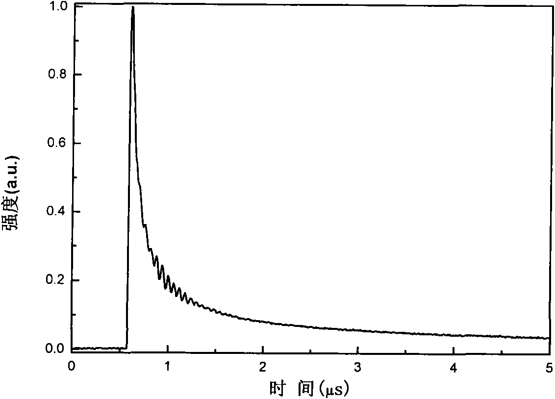
[0020] A method for making a fast-response ultraviolet detector of an n-type doped ZnO thin film, the method comprising the following steps:
[0021] Step 1, clean the quartz substrate with acetone, ethanol and deionized water;
[0022] Step 2, on the cleaned quartz substrate, grow a Ga-doped ZnO thin film with a thickness of 500nm with a magnetron sputtering device, and its composition ratio is Ga 2 o 3 : ZnO=1wt%: 99wt%;
[0023] Step 3, annealing the grown Ga-doped ZnO film in oxygen at an annealing temperature of 830°C;
[0024] Step 4, on the annealed Ga-doped ZnO thin film, two Al electrodes with a thickness of 140 nm are evaporated using a thermal evaporation device, and the distance between the two Al electrodes is 200 microns.
[0025] The structures fabricated by the above steps are, from bottom to top, a quartz substrate, a Ga-doped ZnO thin film, and a fast-response ultraviolet detector of two Al electrodes with n-type doped ZnO thin films.
Embodiment approach 2
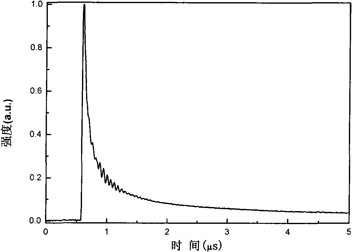
[0027] A method for making a fast-response ultraviolet detector of an n-type doped ZnO thin film, the method comprising the following steps:
[0028] Step 1, the quartz substrate is cleaned with hydrochloric acid, ethanol, and deionized water;
[0029] Step 2, on the cleaned quartz substrate, grow a Ga-doped ZnO thin film with a thickness of 1000 nm with a magnetron sputtering device, and its composition ratio is Ga 2 o 3 : ZnO=3wt%: 97wt%;
[0030] Step 3, annealing the grown Ga-doped ZnO film in oxygen at an annealing temperature of 700°C;
[0031] Step 4, on the annealed Ga-doped ZnO thin film, two Al electrodes with a thickness of 100 nm are evaporated using a magnetron sputtering device, and the distance between the electrodes is 5 microns.
[0032] The structures fabricated by the above steps are, from bottom to top, a quartz substrate, a Ga-doped ZnO thin film, and a fast-response ultraviolet detector of two Al electrodes with n-type doped ZnO thin films.
Embodiment approach 3
[0034] A method for making a fast-response ultraviolet detector of an n-type doped ZnO thin film, the method comprising the following steps:
[0035] Step 1, clean the quartz substrate with acetone, ethanol, isopropanol;
[0036] Step 2, on the cleaned quartz substrate, grow a Ga-doped ZnO thin film with a thickness of 1200nm with a magnetron sputtering device, and its composition ratio is Ga 2 o 3 : ZnO=0.5wt%: 99.5wt%;
[0037] Step 3, anneal the grown Ga-doped ZnO film in oxygen at a temperature of 900° C.; Step 4, use thermal evaporation equipment to vapor-deposit two Al particles with a thickness of 200 nm on the annealed Ga-doped ZnO film. Electrodes, the distance between two Al electrodes is 2000 microns.
[0038] The structure fabricated by the above steps is sequentially from bottom to top: a quartz substrate, a Ga-doped ZnO thin film, and a fast-response ultraviolet detector of Ga-doped ZnO thin films with two Al electrodes.
[0039] The n-type doped ZnO film in ...
PUM
| Property | Measurement | Unit |
|---|---|---|
| Thickness | aaaaa | aaaaa |
| Thickness | aaaaa | aaaaa |
Abstract
Description
Claims
Application Information
 - R&D
- Intellectual Property
- Life Sciences
- Materials
- Tech Scout
- Unparalleled Data Quality
- Higher Quality Content
- 60% Fewer Hallucinations
Browse by: Latest US Patents, China's latest patents, Technical Efficacy Thesaurus, Application Domain, Technology Topic, Popular Technical Reports.
© 2025 PatSnap. All rights reserved.Legal|Privacy policy|Modern Slavery Act Transparency Statement|Sitemap|About US| Contact US: help@patsnap.com


