Palladium-doped carbon film material with photovoltaic effect
A photovoltaic effect, carbon thin film technology, applied in photovoltaic power generation, sustainable manufacturing/processing, electrical components, etc., can solve the problem that single-walled carbon nanotubes are expensive and limit the application of single-walled carbon nanotubes/silicon heterojunction solar cells and development and other issues, to achieve the effect of abundant reserves, good application value and stable nature
- Summary
- Abstract
- Description
- Claims
- Application Information
AI Technical Summary
Problems solved by technology
Method used
Image
Examples
Embodiment 1
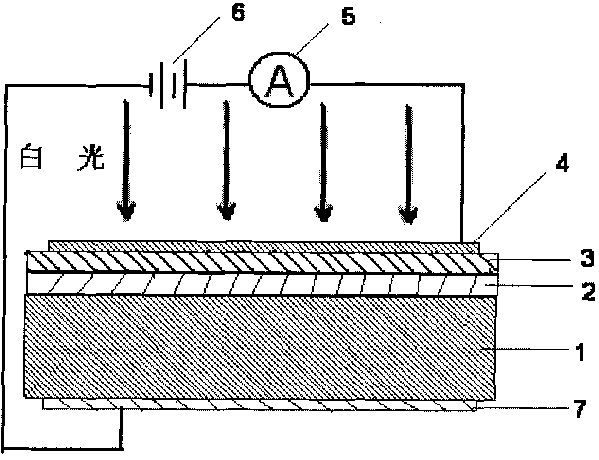
[0024] Example 1, take graphite powder with a purity of 99.9%, mix it with palladium powder with a purity of 99.9%, and make a palladium-carbon composite target with a palladium atomic number content of 1% by cold pressing. The palladium-carbon composite target is sputtered onto a silicon wafer 1 with a thickness of 1.0 mm to retain a natural oxide layer 2 by magnetron sputtering. The thickness of silicon dioxide 2 is about 1.2 nanometers, forming a silicon wafer on the silicon wafer. A palladium-doped carbon film 3 with a layer thickness of 100 nanometers is sputtered with a semi-transparent copper film 4 on the palladium-doped carbon film 3, the copper film 4 is used as an upper electrode, and 7 is an indium back electrode. Connect the DC power supply 6 on the semiconductor-oxide-semiconductor (SIS) structure material, and the ammeter 5 becomes an SIS structure with photovoltaic effect, such as figure 1 shown. The sputtering DC voltage was 0.40 kV, the sputtering DC current...
Embodiment 2
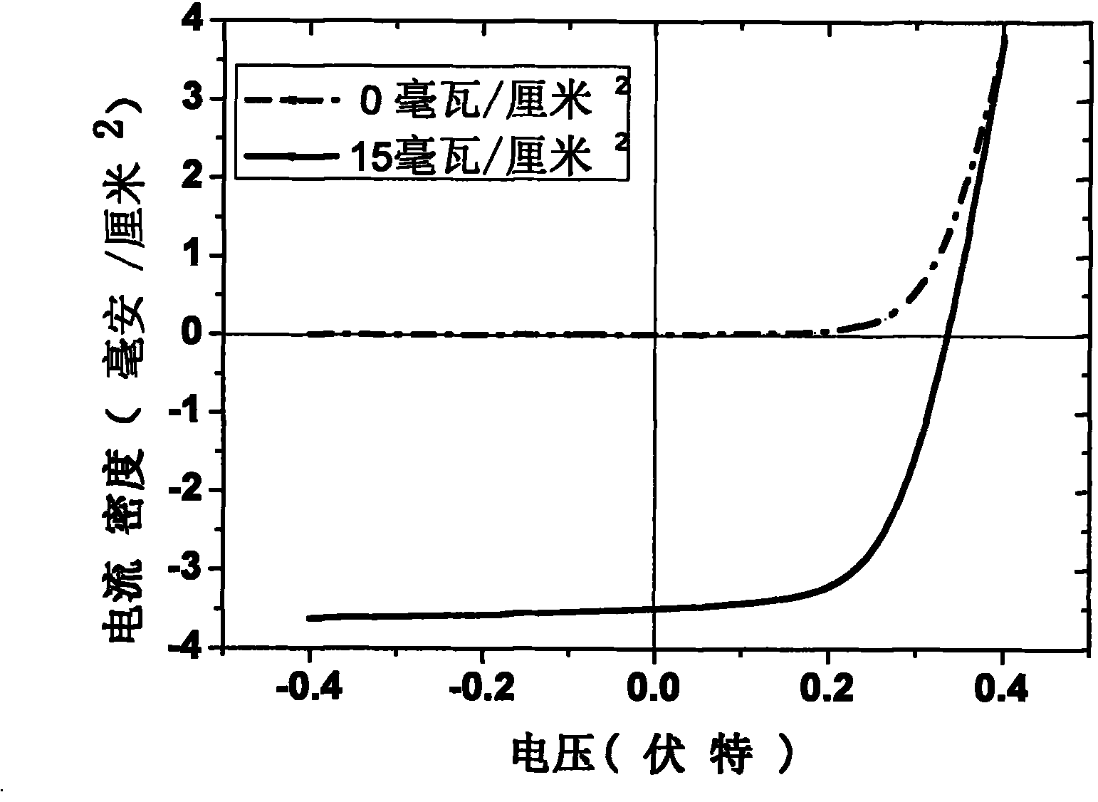
[0025] Example 2, take graphite powder with a purity of 99.9%, mix it with palladium powder with a purity of 99.9%, and make a palladium-carbon composite target with a palladium atomic number content of 2% by cold pressing. The palladium-carbon composite target is sputtered onto a silicon wafer 1 with a thickness of 1.0 mm by magnetron sputtering, and a palladium-doped carbon film 3 with a thickness of 100 nanometers is formed on the silicon wafer. 3 is sputtered with a layer of translucent copper film 4, the copper film 4 is used as an upper electrode, and 7 is an indium back electrode. Connect the DC power supply 6 on the heterojunction material, and the ammeter 5 becomes a heterojunction with photovoltaic effect, such as image 3shown. The sputtering DC voltage was 0.40 kV, the sputtering DC current was 0.12 A, the sputtering deposition temperature was 350° C., and the sputtering time was 90 minutes. mW / cm on sample at room temperature 2 The current density-voltage chara...
PUM
| Property | Measurement | Unit |
|---|---|---|
| Thickness | aaaaa | aaaaa |
| Thickness | aaaaa | aaaaa |
| Thickness | aaaaa | aaaaa |
Abstract
Description
Claims
Application Information
 - R&D
- Intellectual Property
- Life Sciences
- Materials
- Tech Scout
- Unparalleled Data Quality
- Higher Quality Content
- 60% Fewer Hallucinations
Browse by: Latest US Patents, China's latest patents, Technical Efficacy Thesaurus, Application Domain, Technology Topic, Popular Technical Reports.
© 2025 PatSnap. All rights reserved.Legal|Privacy policy|Modern Slavery Act Transparency Statement|Sitemap|About US| Contact US: help@patsnap.com


