Semiconductor package and method of packaging the same

A packaging method and semiconductor technology, applied in semiconductor/solid-state device manufacturing, semiconductor devices, semiconductor/solid-state device components, etc., can solve problems such as easy oxidation of copper, failure of copper ball 24 spherical shape, high electric burning temperature, etc.

Active Publication Date: 2010-08-11
ADVANCED SEMICON ENG INC
View PDF0 Cites 7 Cited by
  • Summary
  • Abstract
  • Description
  • Claims
  • Application Information

AI Technical Summary

Problems solved by technology

[0005] However, in the electric firing process of the copper ball 24, due to the high electric firing temperature, the copper is prone to oxidation, which in turn causes the spherical failure of the copper ball 24 (that is, non-spherical shape)

Method used


Image

  • Semiconductor package and method of packaging the same
  • Semiconductor package and method of packaging the same
  • Semiconductor package and method of packaging the same

Examples


Embodiment Construction

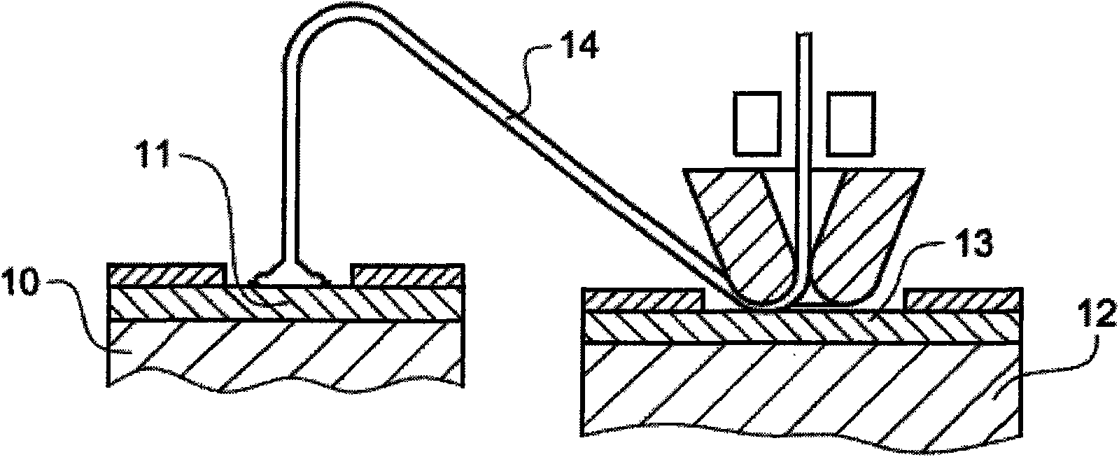
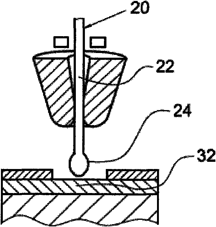
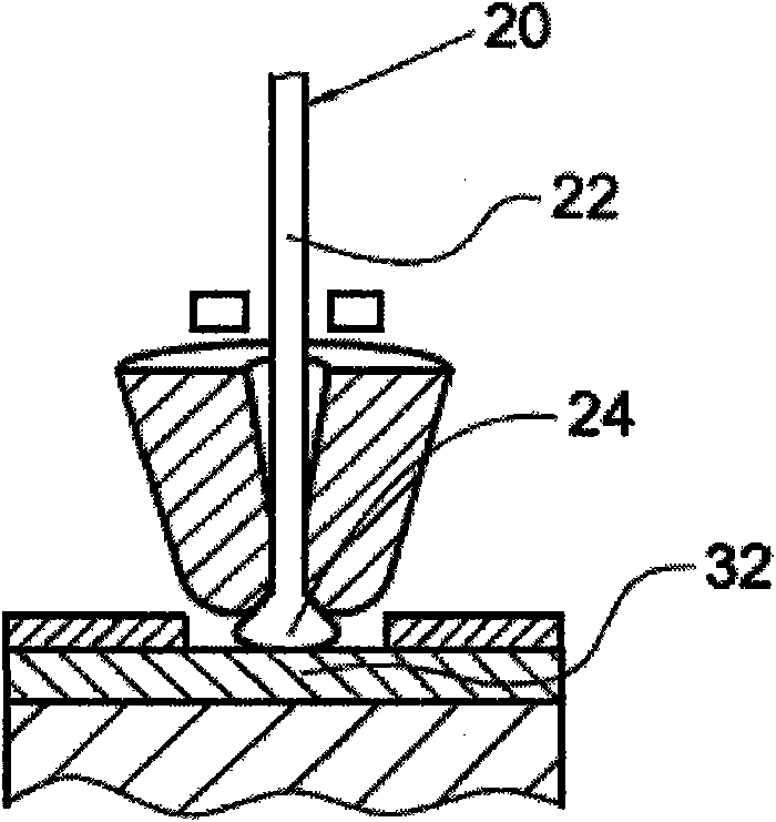
[0054] refer to Figure 5 to Figure 12 , which shows an embodiment of the semiconductor packaging method of the present invention. refer to Figure 5, providing a carrier 112 having an upper surface 113 and a lower surface 114 opposite thereto. On the upper surface of the carrier 112 is arranged a wafer 110 , wherein the wafer 110 has an active surface 115 and a rear surface 116 opposite thereto. Pads 132 (such as aluminum pads) are disposed on the active surface 115 of the die 110 . refer to Figure 6 , in this embodiment, the brazing wire 120 is provided by the wire bonding machine 102 , and the brazing wire 120 includes the linear portion 122 . refer to Figure 7 , make the inert gas 140 pass around the wire end 123 of the linear portion 122, and pass through an electric firing process, such as a discharge process of an electronic burning ball device (electrical flame-off; EFO) 104 with high voltage, to The wire end 123 of the wire portion 122 forms a spherical portio...


PUM


Abstract

The invention relates to a semiconductor package and a method of packaging the same, wherein the method comprises the following steps: setting wafers on a bearing piece; inert gas passing through the periphery of the line end of the linear part of the copper welding wire so that the line end is formed into a ball part, wherein the distance between each edge of the ball part and the central line of the copper welding wire is basically equal, and the linear part and the ball part respectively have a line diameter D1 and a ball diameter D2, and D2 is larger than or equal to 2*D1 and is smaller than or equal to 2.5*D1; bonding the ball part to the pad of the wafer, wherein the ball part is formed into arc bonding part after bonding, the distance between each edge of the arc bonding part and the central line of the copper welding wire is basically equal, the linear part after bonding has a cross section diameter D1', the arc bonding part has a cross section diameter D2', and D2' is larger than or equal to 1.8*D1' and is smaller than or equal to 3*D1'; and coating the wafer and the copper welding wire and covering the bearing piece so that a sealing compound, the wafer and the bearing piece form the package. In the electric burning process of the ball part of the copper welding wire in the method of packaging the semiconductor, the inert gas can efficiently prevent oxygen gas from being contacted with copper, thus copper is not easy to oxidize even at high electric burning temperature; therefore, the invention has the benefit that the ball part is in the shape of a ball successfully.

Description

technical field [0001] The invention relates to a semiconductor packaging method and a wire bonding process of the semiconductor packaging method. Background technique [0002] refer to figure 1 In the manufacturing process of the semiconductor package, the technology of the wire bonding method widely applies the wire bonding 14 to the electrical connection between the pads 11 of the chip 10 and the pads 13 of the substrate 12 . The wire bonding process is mainly based on gold wires, but copper wires have the advantage of low cost. Compared with gold, copper has better electrical and thermal conductivity, which can make the wire diameter of the copper bonding wire smaller and the heat dissipation efficiency is better. However, copper has the disadvantages of insufficient ductility and easy oxidation, which still limits the application of copper wires. [0003] At present, copper bonding wires can only be applied to large-sized die pads or die pads of low-k material (low-K...

Claims


Application Information

Patent Timeline
Patent Type & Authority Applications(China)
IPC IPC(8): H01L23/482H01L23/49H01L21/60
CPCH01L2924/01046H01L2924/01082H01L2224/4824H01L2224/05624H01L24/78H01L2224/32245H01L2224/32014H01L24/85H01L2224/73215H01L2924/15311H01L2924/01029H01L2924/01028H01L2224/48091H01L2924/01013H01L2224/45147H01L2224/32225H01L2224/92247H01L2224/85H01L24/48H01L2224/78301H01L2924/01047H01L2924/01079H01L2224/48465H01L2224/48247H01L24/45H01L2224/48227H01L2224/48455H01L2924/01074H01L2224/48228H01L2924/01011H01L2224/73265H01L2224/48799H01L2224/45015H01L2924/181H01L2224/85205H01L24/73H01L2224/45565H01L2224/45144H01L2224/48H01L2224/02166H01L2924/00011H01L2224/45H01L2224/78H01L2924/00014H01L2924/00H01L2924/00012H01L2224/48824H01L2924/207H01L2224/45664H01L2924/01005H01L2924/00015
Inventor 黄文彬徐正宗曾正男洪志成
Owner ADVANCED SEMICON ENG INC
Why Eureka
Try Eureka