
Windowing-type semiconductor packaging member and manufacture method thereof

A technology for semiconductors and packages, which is applied in the field of windowed semiconductor packages and its manufacturing methods, can solve the problems of shortening the arc length of welding wires, being unable to apply, reducing the electrical connection path between chips and conductive trace layers, etc., to achieve shortening The arc length of the welding wire, the improvement of the circuit layout and the quality of the electrical connection, and the effect of overcoming the short circuit

Active Publication Date: 2010-06-16
SILICONWARE PRECISION IND CO LTD
View PDF10 Cites 4 Cited by
  • Summary
  • Abstract
  • Description
  • Claims
  • Application Information

AI Technical Summary

Problems solved by technology

[0006] This kind of package does not need to use a base (such as a prefabricated lead frame, substrate, etc.) as a chip carrier, which can reduce the manufacturing cost of the semiconductor package. The distribution of the pads is elastically arranged and can go deep into the layout area of ​​the bonding wire connected to the chip, so as to effectively shorten the arc length of the bonding wire used to electrically connect the chip to the terminal of the conductive trace layer, and reduce the chip and the conductive trace layer. The electrical connection path between layers, but the manufacturing method of the above-mentioned package cannot be applied to a window-type semiconductor package with a center-pad (center-pad) dynamic random access memory (Dynamic Random Access Memory, DRAM) chip. middle

Method used


Image

  • Windowing-type semiconductor packaging member and manufacture method thereof
  • Windowing-type semiconductor packaging member and manufacture method thereof
  • Windowing-type semiconductor packaging member and manufacture method thereof

Examples


no. 1 example

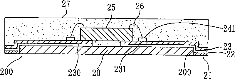
[0073] see Figure 3A to Figure 3K Shown is a schematic diagram of the first embodiment of the method for manufacturing a window-type semiconductor package of the present invention, wherein, Figure 3C for Figure 3B a schematic cross-section of the Figure 3G for Figure 3F sectional schematic diagram.

[0074] like Figure 3A to Figure 3C As shown, a metal (such as copper) base plate 310 is provided to form a dielectric layer 311 with a thickness of 50 to 100 microns (μm) on the metal base plate 310, and an exposed part of the metal is formed on the dielectric layer 311. The first opening 305 of the bottom plate 310 , and a plurality of first conductive vias 303 and second conductive vias 304 exposing part of the metal bottom plate 310 are formed on both sides of the first opening 305 .

[0075] like Figure 3D to Figure 3E As shown, the first conductive via 303 and the second conductive via 304 are filled with a conductive material 320 such as gold / nickel / copper (Au / N...

no. 2 example

[0085] see Figure 4A to Figure 4I Shown is a schematic diagram of the second embodiment of the method for manufacturing a window-type semiconductor package of the present invention, wherein, Figure 4C for Figure 4B a schematic cross-section of the Figure 4G for Figure 4F sectional schematic diagram. In addition, in order to simplify the drawings and facilitate understanding, elements corresponding to or similar to those in the foregoing embodiments are denoted by the same numbers. Furthermore, the manufacturing method of the window-type semiconductor package of this embodiment is substantially the same as that of the first embodiment, the main difference being that the first opening 305 can be formed on the dielectric substrate 300 by punching or laser cutting.

[0086] like Figure 4A to Figure 4C As shown, a metal base plate 310 is provided to form a dielectric layer 311 with a thickness of 50 to 100 microns (μm) on the metal base plate 310, and a plurality of firs...

no. 3 example

[0092] see also Figure 5A to Figure 5I , is a schematic diagram of the third embodiment of the manufacturing method of the window-type semiconductor package of the present invention, wherein, Figure 5B for Figure 5A a schematic cross-section of the Figure 5E for Figure 5D sectional schematic diagram. In addition, in order to simplify the drawings and facilitate understanding, elements corresponding to or similar to those in the foregoing embodiments are denoted by the same numbers. Furthermore, the manufacturing method of the window-type semiconductor package of this embodiment is substantially the same as that of the first embodiment, the main difference is that the conductive trace layer 330 of the dielectric carrier 300 is embedded in the dielectric carrier 300 .

[0093] like Figure 5A to Figure 5B As shown, a metal base plate (such as copper) 310 is provided, a resistive layer 332 is formed on the metal base plate 310 , and a plurality of third openings 335 exp...


PUM


Abstract

The invention relates to windowing-type semiconductor packaging member and manufacture method thereof. The manufacture method mainly comprises the following steps of: arranging a first opening on a dielectric support plate with a first surface and a second surface, arranging a first conductive through hole and a second conductive through hole at two sides of the first opening so as to form a conductive trace layer on the first surface of the dielectric support plate, wherein the conductive trace layer is used for electrically connecting conducting materials in the first conductive through hole and the second conductive through hole; connecting a chip to the conductive trace layer, exposing a chip pad of the chip out of the first opening so as to electrically connect the chip pad of the chip to the conductive material of the first conductive through hole on the second surface of the dielectric support plate by using a plurality of welding wires through the first opening; and planting awelding ball on the conductive material of the second conductive through hole of the second surface of the dielectric support plate.

Description

technical field [0001] The invention relates to a semiconductor package and its manufacturing method, in particular to a window-opened semiconductor package and its manufacturing method. Background technique [0002] Window Ball Grid Array (Window Ball Grid Array) semiconductor package is to open at least one through hole through the substrate on the substrate used, so that the chip can be placed on a surface of the substrate in a way to cover the through hole. , and use the bonding wires passing through the through hole to electrically connect the chip and the substrate, and plant a plurality of solder balls on the other opposite surface of the substrate, so as to connect the chip to external electronic components. Therefore, it can thus It is designed to shorten the bonding wire length of the Central-Pad Type chip to reduce the transmission impedance of telecommunications, thereby improving its electrical performance and reducing the thickness of the overall package. [0...

Claims


Application Information

Patent Timeline
Patent Type & Authority Applications(China)
IPC IPC(8): H01L21/50H01L21/60H01L21/56H01L23/488H01L23/498H01L23/13H01L23/31
CPCH01L2924/15311H01L2224/4824H01L2924/3011H01L2924/01079H01L2224/48091H01L2224/73215H01L2224/32225H01L2924/181H01L2924/00014H01L2924/00H01L2924/00012
Inventor 黄致明张正易林介源黄建屏柯俊吉
Owner SILICONWARE PRECISION IND CO LTD
Learn More