Process for manufacturing surface channel PMOS device with polycide

A technology of surface trenches and manufacturing processes, applied in semiconductor/solid-state device manufacturing, electrical components, circuits, etc., can solve problems such as low leakage current, achieve low leakage, simple process, and reduce device size

Active Publication Date: 2010-06-16
SHANGHAI HUAHONG GRACE SEMICON MFG CORP
View PDF0 Cites 8 Cited by
  • Summary
  • Abstract
  • Description
  • Claims
  • Application Information

AI Technical Summary

Problems solved by technology

The biggest disadvantage of buried channel devices is that they must have a higher threshold voltage to have a lower leakage current

Method used


Image

  • Process for manufacturing surface channel PMOS device with polycide
  • Process for manufacturing surface channel PMOS device with polycide
  • Process for manufacturing surface channel PMOS device with polycide

Examples


Embodiment Construction

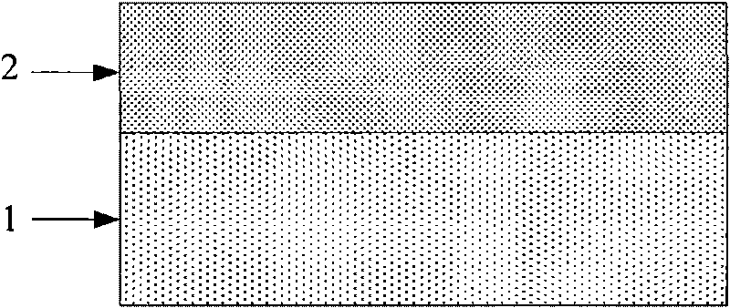
[0017] The fabrication process of the surface channel PMOS device with polysilicon in the present invention usually has a field oxygen isolation, LOCOS isolation or shallow trench isolation (STI) process before the process starts, which is used to isolate the active regions on the silicon wafer from each other. On this basis, the present invention also comprises the following steps:

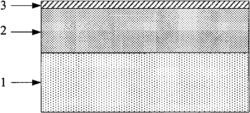
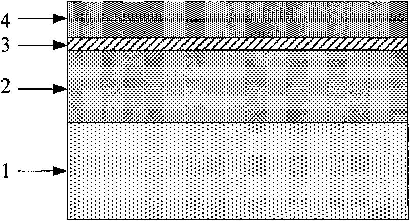
[0018] Step 1, see Figure 1a , doping N-type impurities on the P-type silicon substrate 1 to form an N-type channel 2 . Commonly used N-type impurities include phosphorus, arsenic, antimony, and the like. The doping method can be thermal diffusion or ion implantation.

[0019] After the N-type channel 2 is formed, threshold voltage adjustment implantation (not shown) can also be performed. That is to inject N-type or P-type impurities into the N-type channel 2 to change the impurity concentration of the N-type channel 2 . Since the threshold voltage of the MOS device is very sensitive to the...


PUM


Abstract

The invention discloses a process for manufacturing a surface channel PMOS device with polycide, which comprises the following steps of: 1, doping an N-type impurity on a P-type silicon substrate to form an N-type channel; 2, depositing a layer of oxidized silicon nitride on the surface of a silicon wafer; 3, depositing a layer of polysilicon on the surface of the silicon wafer and doping a P-type impurity in a gate region of the layer of polysilicon to form P-type polysilicon; 4, forming the polycide on the surface of the silicon wafer; 5, etching the polycide, the P-type polysilicon and the oxidized silicon nitride except for the polycide, the P-type polysilicon and the oxidized silicon nitride outside the gate region until the N-type channel is exposed; 6, depositing a layer of silicon nitride on the surface of the silicon wafer and etching the layer of silicon nitride until the N-type channel is exposed and part of silicon nitride side wall is reserved on the side wall of the P-type polysilicon; and 7, performing ion implantation of the P-type impurity on the silicon wafer to form a source region and a drain region of the PMOS device. The surface channel PMOS device manufactured by the invention can realize low leakage of electricity under a lower threshold voltage.

Description

technical field [0001] The invention relates to a manufacturing process of a semiconductor device, in particular to a manufacturing process of a PMOS device. Background technique [0002] In semiconductor integrated circuits with a size of 0.35 μm and above, polysilicon gates of MOS devices are usually covered with polycide. Polysilicon is formed by the reaction of refractory metals and polysilicon. Refractory metals include cobalt, molybdenum, platinum, tantalum, titanium, tungsten, etc. During the formation of the polysilicon, the silicon oxide remaining on the silicon surface will be reduced, thereby reducing the contact resistance of the polysilicon gate. [0003] The polysilicon compound covers the polysilicon gate, and its dense characteristics make it impossible for ions to be implanted into the polysilicon gate during the source-drain implantation of the MOS device. In this way, the doping of the polysilicon gate can only be done in-situ when the polysilicon is dep...

Claims


Application Information

Patent Timeline
Patent Type & Authority Applications(China)
IPC IPC(8): H01L21/336
Inventor 钱文生
Owner SHANGHAI HUAHONG GRACE SEMICON MFG CORP
Why Eureka
Try Eureka