Manufacturing method of wafer level glass microcavity used for packaging MEMS
A manufacturing method and glass micro technology, applied in the field of MEMS manufacturing, can solve problems such as complex methods, and achieve the effects of simple methods, avoiding complex processes, and avoiding high energy and high costs.
- Summary
- Abstract
- Description
- Claims
- Application Information
AI Technical Summary
Problems solved by technology
Method used
Image
Examples
Embodiment 1
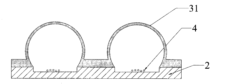
[0029] A method for manufacturing a wafer-level glass microcavity for MEMS packaging, comprising the following steps:
[0030]The first step utilizes Si micromachining process to etch shallow grooves on Si wafers (such as 4-inch wafers), and the silicon wafers used can be silicon wafers of standard thickness, such as 500 micron thick silicon wafers. The depth is 10-200 microns, such as 15 microns, 30 microns, 40 microns, 60 microns, 95 microns, 132 microns, 150 microns, 180 microns, and the aspect ratio is usually less than 2, such as 1.5, 1, 0.8, 0.5, 0.2, 0.1, 0.05, 0.02, the micromachining process of the pattern structure on the Si wafer is a wet etching process, or a dry inductively coupled plasma (ICP) etching process, or reactive ion etching, A wet etching process is preferred, such as etching with a TMAH solution, and the pattern can be a square or circular groove array (for packaging MEMS device arrays),
[0031] The second step is to place an appropriate amount of hi...
Embodiment 2
[0036] A method for manufacturing a wafer-level glass microcavity for MEMS packaging, comprising the following steps:
[0037] The first step is to use Si micromachining technology to etch shallow grooves on a 4-inch Si wafer. The silicon wafer used can be a standard thickness silicon wafer with a thickness of 500 microns. The depth of the shallow grooves is 60 microns. It is a circular groove of 2 mm, the micromachining process of the pattern structure on the Si wafer is a wet etching process, the etching solution used is TMAH solution, the concentration is 10%, and the temperature is 80 degrees Celsius.
[0038] In the second step, chemically pure calcium carbonate powder is placed in a shallow tank with a particle size of 5 microns and a mass of 2 micrograms.
[0039] The 3rd step, above-mentioned Si disc and Pyrex7740 glass disc (a kind of brand of borosilicate glass, the U.S. Corning-corning company produces, the market can buy, usually through polishing, its size is iden...
Embodiment 3
[0044] A method for manufacturing a wafer-level glass microcavity for MEMS packaging, comprising the following steps:
[0045] The first step is to use Si micromachining technology to etch shallow grooves on a 4-inch Si wafer. The silicon wafer used can be a silicon wafer of standard thickness with a thickness of 500 microns. The depth of the shallow grooves is 100 microns. It is a circular groove of 2 mm, the micromachining process of the pattern structure on the Si wafer is a wet etching process, the etching solution used is TMAH solution, the concentration is 10%, and the temperature is 80 degrees Celsius.
[0046] In the second step, chemically pure calcium carbonate powder is placed in a shallow tank with a particle size of 5 microns and a mass of 4 micrograms.
[0047] The 3rd step, above-mentioned Si disc and Pyrex7740 glass disc (a kind of brand of borosilicate glass, the U.S. Corning-corning company produces, the market can buy, usually through polishing, its size is ...
PUM
 Abstract
Description
Claims
Application Information
 - R&D
- Intellectual Property
- Life Sciences
- Materials
- Tech Scout
- Unparalleled Data Quality
- Higher Quality Content
- 60% Fewer Hallucinations
Browse by: Latest US Patents, China's latest patents, Technical Efficacy Thesaurus, Application Domain, Technology Topic, Popular Technical Reports.
© 2025 PatSnap. All rights reserved.Legal|Privacy policy|Modern Slavery Act Transparency Statement|Sitemap|About US| Contact US: help@patsnap.com


