Preparation method of solar micro battery on basis of directional carbon nano tube
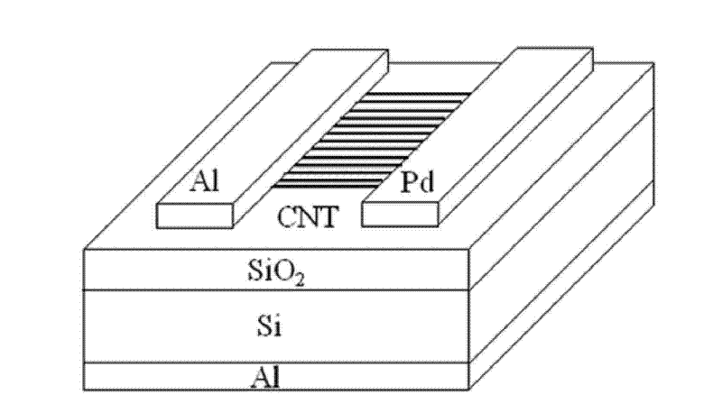
A solar micro-battery and carbon nanotube technology, which is applied in the manufacture of circuits, electrical components, and final products, can solve problems such as unstable contact, large contact resistance, and reduced electron collection efficiency of electrodes to achieve high stability and simple effect
- Summary
- Abstract
- Description
- Claims
- Application Information
AI Technical Summary
Problems solved by technology
Method used
Image
Examples
Embodiment 1
[0023] In this example, an aligned single-walled carbon nanotube film was obtained by using an alternating electric field two-dimensional electrophoresis method. The single-walled carbon nanotubes were placed in chloroform and dispersed under ultrasonic waves with a frequency of 30KHz for 2 minutes to form a stable dispersed carbon nanotube suspension.
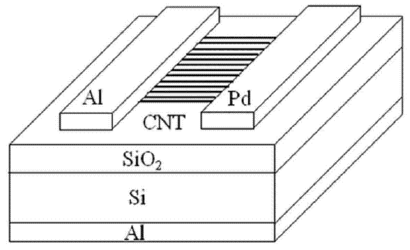
[0024] On a silicon wafer containing a 200nm-thick silicon dioxide insulating layer, ultraviolet-visible light lithography technology is used to fabricate parallel and opposite metal Pd and Al electrode pair patterns, with a pitch of 1 μm and a relative width of 10 μm. Use metal Pd as the metal electrode with high work function and Al as the metal electrode with low work function, and apply a high-frequency sinusoidal AC voltage with a frequency of 5 MHz and a field strength of 10 V / Ω between the two electrodes. A suspension of carbon nanotubes with a concentration of 0.5 μg / mL was added dropwise on the two electrodes for dire...
Embodiment 2
[0028] In this example, an aligned single-walled carbon nanotube film was obtained by using an alternating electric field two-dimensional electrophoresis method. The single-walled carbon nanotubes were placed in isopropanol, and dispersed under ultrasonic waves with a frequency of 30KHz for 2 minutes to form a stable dispersed single-walled carbon nanotube suspension.
[0029] On a silicon wafer containing a 200nm-thick silicon dioxide insulating layer, ultraviolet-visible light lithography technology is used to fabricate parallel and opposite metal Pt and Al electrode pair patterns, with a spacing of 10 μm and a relative width of 100 μm. Between the two electrodes, apply a high-frequency sinusoidal AC voltage with a frequency of 15MHz and a field strength of 20V / μm. A suspension of single-walled carbon nanotubes with a concentration of 0.1 μg / mL was dropped on the two electrodes to cause directional deposition under the action of an alternating electric field. The deposition ...
Embodiment 3
[0033] In this example, an aligned single-walled carbon nanotube film was obtained by using an alternating electric field two-dimensional electrophoresis method. The single-walled carbon nanotubes were placed in chloroform and dispersed under ultrasonic waves with a frequency of 30 KHz for 2 minutes to form a stable dispersed single-walled carbon nanotube suspension.
[0034]On a silicon wafer containing a 500nm-thick silicon dioxide insulating layer, electron beam lithography is used to produce parallel and opposite patterns of metal Ni and Ag electrode pairs, with a spacing of 20 μm and a relative width of 200 μm. Between the two electrodes, apply a high-frequency sinusoidal AC voltage with a frequency of 5MHz and a field strength of 10V / μm. A suspension of single-walled carbon nanotubes with a concentration of 0.5 μg / mL was dropped on the two electrodes to cause directional deposition under the action of an alternating electric field. The deposition time was 40 s and the de...
PUM
| Property | Measurement | Unit |
|---|---|---|
| concentration | aaaaa | aaaaa |
| thickness | aaaaa | aaaaa |
| thickness | aaaaa | aaaaa |
Abstract
Description
Claims
Application Information
 - R&D
- Intellectual Property
- Life Sciences
- Materials
- Tech Scout
- Unparalleled Data Quality
- Higher Quality Content
- 60% Fewer Hallucinations
Browse by: Latest US Patents, China's latest patents, Technical Efficacy Thesaurus, Application Domain, Technology Topic, Popular Technical Reports.
© 2025 PatSnap. All rights reserved.Legal|Privacy policy|Modern Slavery Act Transparency Statement|Sitemap|About US| Contact US: help@patsnap.com


