Sn-B plating solution and plating method using it
An electroplating solution, sn-b technology, applied in the field of Sn-B electroplating solution, can solve problems such as shedding, cracks in the electroplating layer, and eutectoid difficulties
- Summary
- Abstract
- Description
- Claims
- Application Information
AI Technical Summary
Problems solved by technology
Method used
Image
Examples
Embodiment 1
[0044] Prepare 15g / L tin sulfate, 30ml / L H 2 SO 4 , 10g / L cresol sulfonic acid, 0.1g / L β-naphthol and 0.1g / L gelatin plating solution.
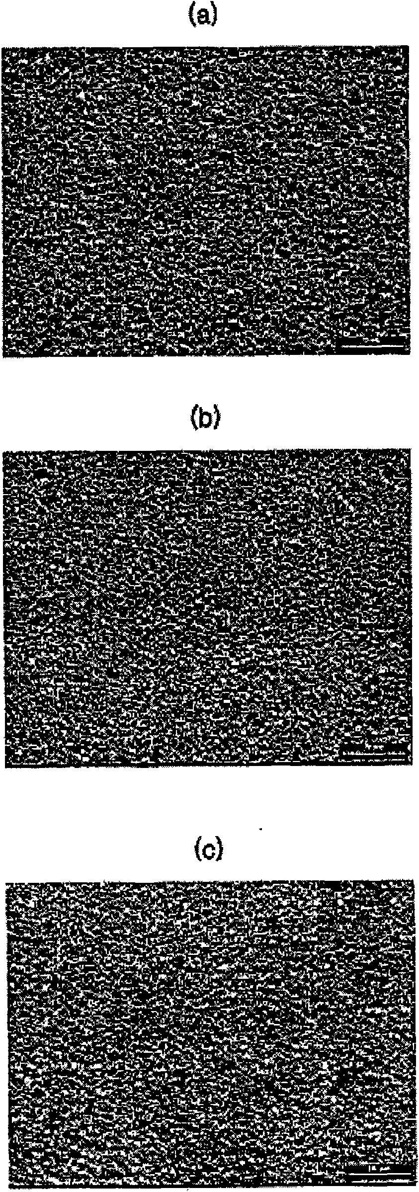
[0045] In experiment 1, 0.1 g / L of DMAB was further added to the plating solution, in experiment 2, 0.5 g / L of DMAB was further added to the plating solution, and in experiment 3, 3 g / L of DMAB was further added to the plating solution. L's DMAB.
[0046] Electroplating is performed under the same electroplating conditions as described above. In other words, the Cu plate is used as the cathode and the soluble Sn is used as the anode, and the current density is 1A / dm 2 , And the plating temperature is room temperature.
[0047] The plating layers of Experiment 1 to Experiment 3 were stored at room temperature for 12 months, and then it was determined whether whiskers were generated on the surface of the plating layer.
[0048] figure 1 (A) to (c) are scanning electron microscope (SEM) photographic images respectively illustrating the surface sta...
Embodiment 2
[0050] Prepare 30g / L tin sulfate, 50ml / L H 2 SO 4 , 20g / L cresol sulfonic acid, 0.3g / L β-naphthol and 0.5g / L gelatin plating solution.
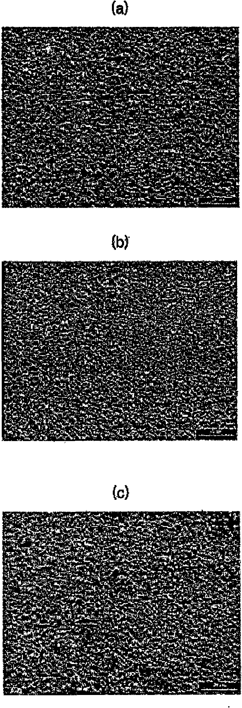
[0051] In experiment 4, 0.1 g / L of DMAB was further added to the plating solution, in experiment 5, 0.5 g / L of DMAB was further added to the plating solution, and in experiment 6, 3 g / L of DMAB was further added to the plating solution. L's DMAB.
[0052] Electroplating was performed under the same electroplating conditions as in Example 1. The plating layers of Experiment 4 to Experiment 6 were stored at room temperature for 12 months, and then it was determined whether whiskers were generated on the surface of the plating layer.
[0053] figure 2 (A) to (c) are SEM photographic images respectively illustrating the surface state of the electroplated layer in Experiment 4 to Experiment 6 after the room temperature storage test.
Embodiment 3
[0055] Prepare 50g / L tin sulfate and 70ml / L H 2 SO 4 , 40g / L cresol sulfonic acid, 0.5g / L β-naphthol and 1.0g / L gelatin plating solution.
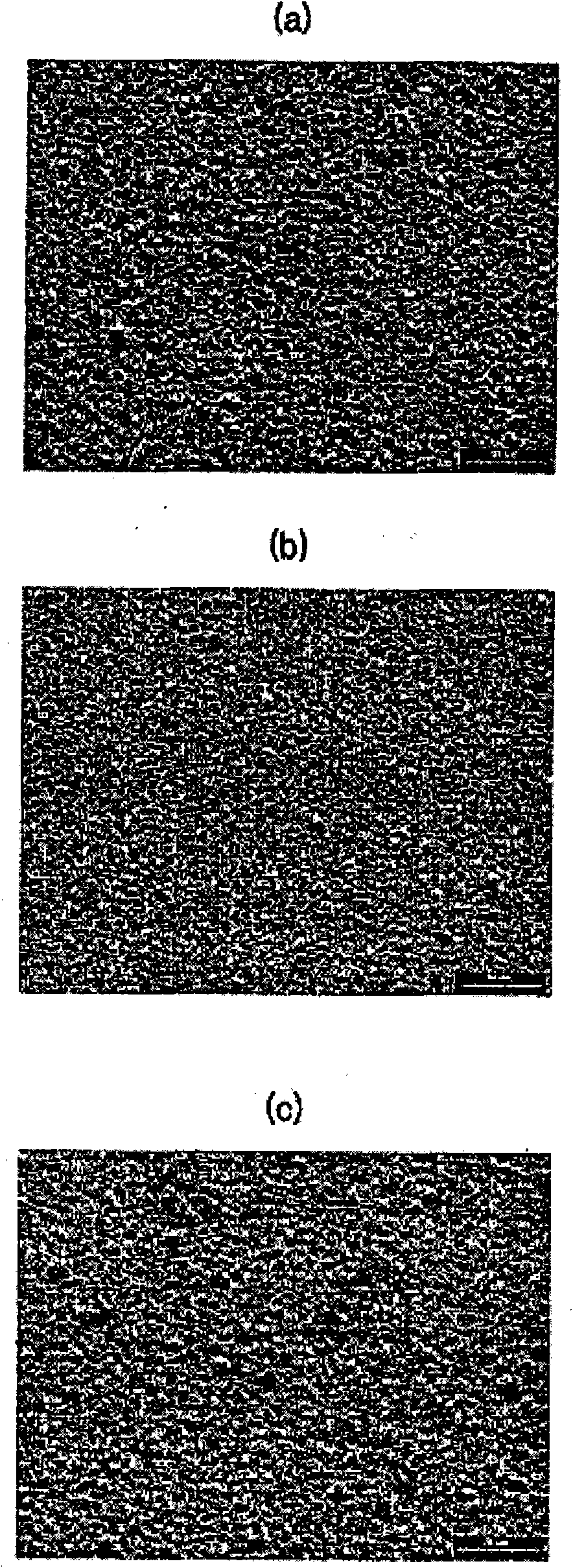
[0056] In experiment 7, 0.1 g / L of DMAB was further added to the plating solution, in experiment 8, 0.5 g / L of DMAB was further added to the plating solution, and in experiment 9, 3 g / L of DMAB was further added to the plating solution. L's DMAB.
[0057] Electroplating was performed under the same electroplating conditions as in Example 1. The plating layers of Experiment 7 to Experiment 9 were stored at room temperature for 12 months, and then it was determined whether whiskers were generated on the surface of the plating layer.
[0058] image 3 (A) to (c) are SEM photographic images respectively illustrating the surface state of the electroplated layer in Experiment 7 to Experiment 9 after the room temperature storage test.
PUM
 Abstract
Description
Claims
Application Information
 - R&D
- Intellectual Property
- Life Sciences
- Materials
- Tech Scout
- Unparalleled Data Quality
- Higher Quality Content
- 60% Fewer Hallucinations
Browse by: Latest US Patents, China's latest patents, Technical Efficacy Thesaurus, Application Domain, Technology Topic, Popular Technical Reports.
© 2025 PatSnap. All rights reserved.Legal|Privacy policy|Modern Slavery Act Transparency Statement|Sitemap|About US| Contact US: help@patsnap.com


