Highly-efficient solar cell
A solar cell and high-efficiency technology, applied in the field of photovoltaic cells, can solve the problems of expensive equipment, high process requirements, and high cost, and achieve the effects of low cost, low production equipment requirements, and improved cost performance
- Summary
- Abstract
- Description
- Claims
- Application Information
AI Technical Summary
Problems solved by technology
Method used
Image
Examples
Embodiment 1
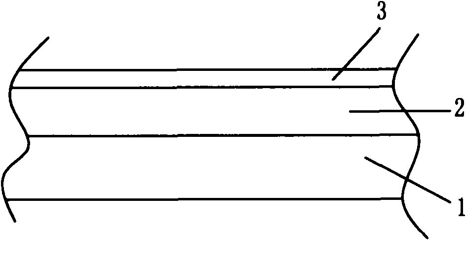
[0026] The structure of the first embodiment of the high-efficiency solar cell of the present invention, such as figure 1 shown. The high-efficiency solar cell has a substrate 1 made of insulating material and a panel 2 made of photoelectric conversion material. The outer surface of the panel 2 is provided with a transparent spectrum conversion film layer 3 containing rare earth fluorescent materials.
[0027] The substrate 1 can be a rigid block, or a rigid sheet, or a flexible film.
[0028] The panel 2 can be made of monocrystalline silicon photoelectric conversion material, or polycrystalline silicon photoelectric conversion material, or amorphous silicon photoelectric conversion material, or copper indium gallium selenium photoelectric conversion material, or cadmium telluride photoelectric conversion material. conversion material, or gallium arsenide photoelectric conversion material, or indium phosphide photoelectric conversion material, or dye-sensitized photoelectr...
Embodiment 2
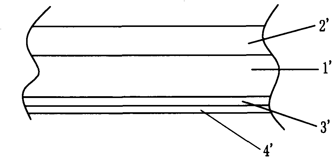
[0046] The structure of the second embodiment of the high-efficiency solar cell of the present invention, such as figure 2 shown. The high-efficiency solar cell has a transparent substrate 1' made of insulating materials and a transparent panel 2' made of photoelectric conversion materials; the outer surface of the substrate 1' is sequentially provided with a transparent spectrum conversion film layer 3' containing rare earth fluorescent materials And reflective layer 4'.
[0047] The substrate 1' can be a rigid block, or a rigid sheet, or a flexible film.
[0048] The panel 2' can be made of monocrystalline silicon photoelectric conversion material, or polycrystalline silicon photoelectric conversion material, or amorphous silicon photoelectric conversion material, or copper indium gallium selenium photoelectric conversion material, or cadmium telluride It is made of photoelectric conversion material, or is made of gallium arsenide photoelectric conversion material, or is ...
PUM
 Abstract
Description
Claims
Application Information
 - R&D
- Intellectual Property
- Life Sciences
- Materials
- Tech Scout
- Unparalleled Data Quality
- Higher Quality Content
- 60% Fewer Hallucinations
Browse by: Latest US Patents, China's latest patents, Technical Efficacy Thesaurus, Application Domain, Technology Topic, Popular Technical Reports.
© 2025 PatSnap. All rights reserved.Legal|Privacy policy|Modern Slavery Act Transparency Statement|Sitemap|About US| Contact US: help@patsnap.com


