Thin film transistor liquid crystal display pixel structure and thin film transistor liquid crystal display array base plate

A liquid crystal display and thin film transistor technology, which is applied in the field of thin film transistor liquid crystal display pixel structures and array substrates, can solve the breakdown of gate scanning lines, cannot protect gate scanning line 1 and data line 2, and cannot obtain release balance, etc. question

Active Publication Date: 2009-11-18
K TRONICS (SUZHOU) TECH CO LTD +1
View PDF0 Cites 9 Cited by
  • Summary
  • Abstract
  • Description
  • Claims
  • Application Information

AI Technical Summary

Problems solved by technology

However, the short-circuit ring (not shown in the figure) is formed in the final process of the TFT LCD array substrate, and cannot protect the gate scanning line 1 and the data line 2 in the previous process. Therefore, the previous process The accumulation of static electricity on the data line 2 and the gate scanning line 1 caused by the substrate handling, cleaning and other process links will not be able to be released and balanced. In actual production, the grid scanning line 1 and the data line 2 often occur Breakdown occurs in the overlapping region 7, even in the channel part (not shown in the figure)
[0005] Once a breakdown occurs in the overlapping area 7, the usual maintenance method is to use a laser (Laser) to cut off part of the data line 2, and then repair the bridge by chemical vapor deposition (CVD), so that the array substrate can be used normally, and the maintenance process is relatively complicated.

Method used


Image

  • Thin film transistor liquid crystal display pixel structure and thin film transistor liquid crystal display array base plate
  • Thin film transistor liquid crystal display pixel structure and thin film transistor liquid crystal display array base plate
  • Thin film transistor liquid crystal display pixel structure and thin film transistor liquid crystal display array base plate

Examples


Embodiment Construction
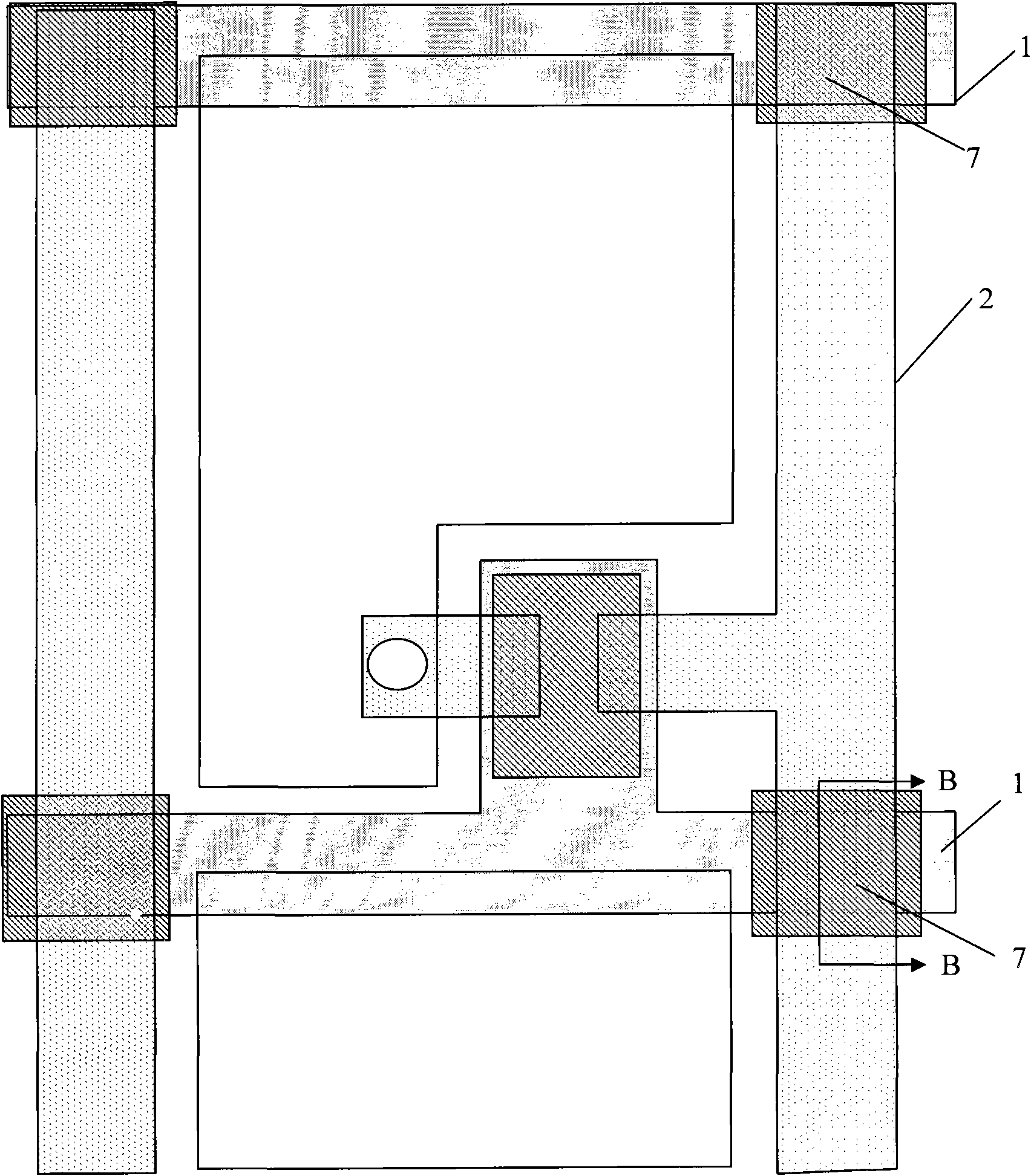
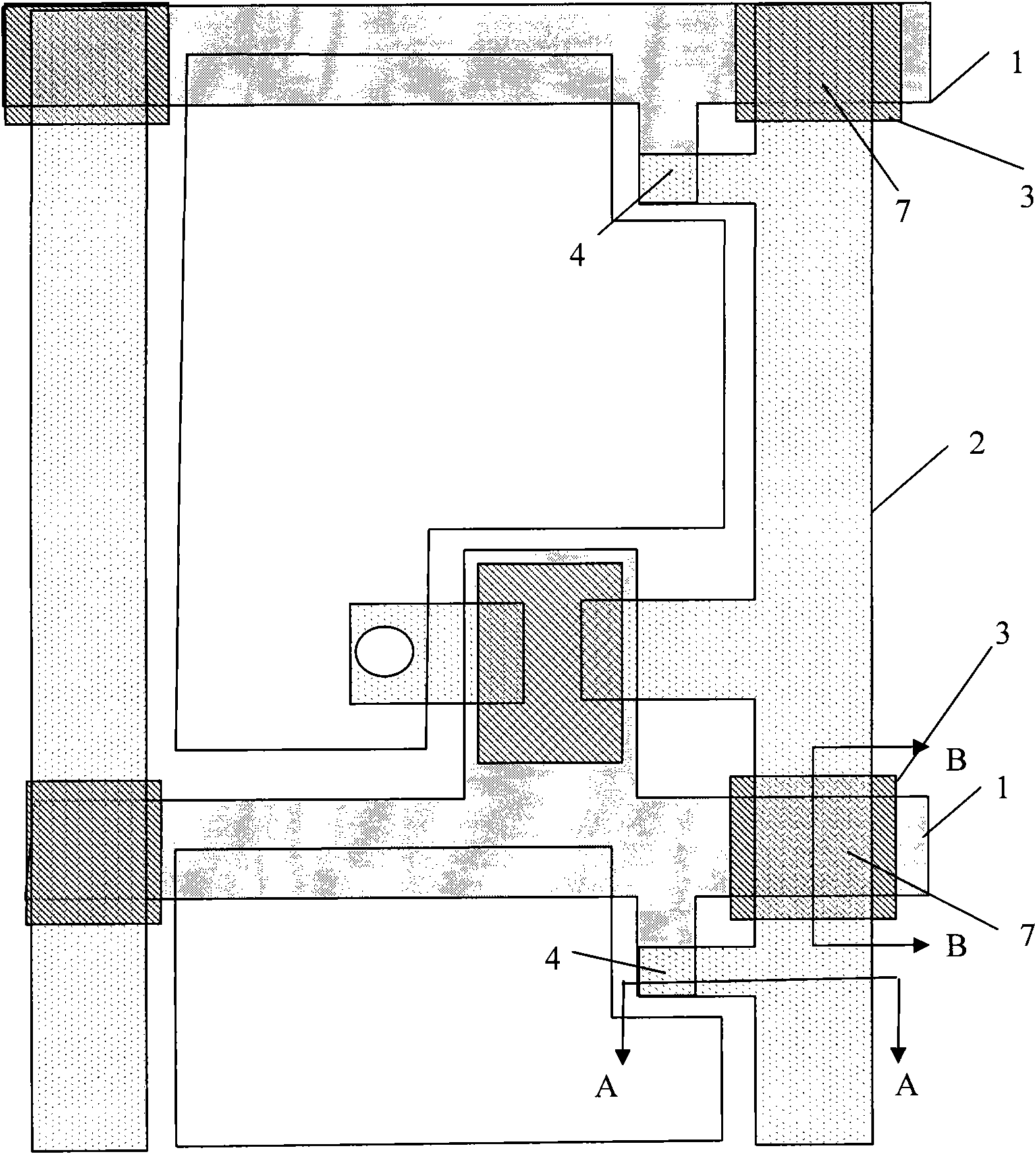
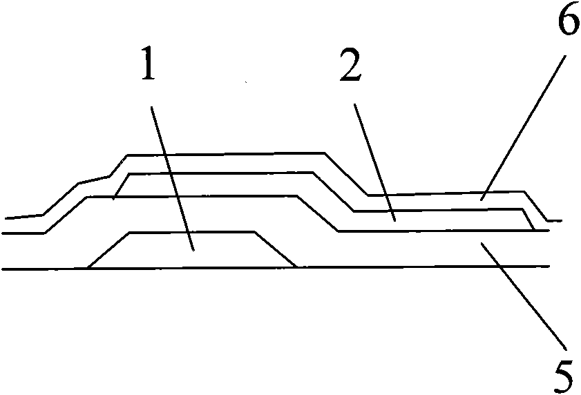
[0026] The basic idea of ​​the present invention is to add a static elimination area near the overlapping area of ​​the data line and the gate scanning line, and in the static elimination area, the metal layer of the gate scanning line and the metal layer of the data line are not connected to each other through the isolation layer.

[0027] Hereinafter, the realization of the TFT LCD pixel structure and the array substrate of the present invention will be described in detail through specific embodiments in conjunction with the accompanying drawings.

[0028] figure 2 It is a schematic diagram of the pixel structure of the TFT LCD array substrate of the present invention, such as figure 2 As shown, two adjacent data lines 2 and two adjacent gate scanning lines 1 overlap each other to define a pixel area, and each pixel structure includes data lines 2, gate scanning lines 1 and the The pixel area, and what kind of structure is included in the specific pixel area belongs to th...


PUM

PropertyMeasurementUnit
thicknessaaaaaaaaaa
thicknessaaaaaaaaaa

Abstract

The invention provides a thin film transistor liquid crystal display pixel structure which comprises a data wire, a grid scanning wire and a pixel area, wherein the data wire and the grid scanning wire are overlapped to form an overlapped area. The thin film transistor liquid crystal display pixel structure is characterized by also comprising an electrostatic elimination area, and the electrostatic elimination area sequentially comprises a grid scanning wire metal layer, an insulating layer and a data wire metal layer, wherein the grid scanning wire metal layer is connected with the grid scanning wire; the insulating layer is used for insulating the grid scanning wire metal layer and the data wire metal layer; and the data wire metal layer is connected with the data wire. The invention also provides a thin film transistor liquid crystal display array base plate. The pixel structure and the array base plate can protect the overlapped area between the grid scanning wire and the data wire and reduce the puncture probability of the overlapped area.

Description

technical field [0001] The invention relates to a thin film transistor (TFT) liquid crystal display (LCD) array substrate, in particular to a thin film transistor liquid crystal display pixel structure and an array substrate. Background technique [0002] At present, the world has entered the era of information revolution, and display technology and display devices occupy a very important position in the development of information technology. Since the flat panel display has the advantages of light weight, thin thickness, small size, no radiation, no flicker, etc., it has become the development direction of display technology. [0003] In flat panel display technology, TFT LCD has the characteristics of low power consumption and no radiation, so it occupies a dominant position in the flat panel display market. [0004] figure 1 It is a schematic diagram of the pixel structure of a traditional TFT LCD array substrate, such as figure 1 As shown, there is an overlapping area...

Claims


Application Information

Patent Timeline
Patent Type & Authority Applications(China)
IPC IPC(8): G02F1/1362H01L27/12
Inventor 彭志龙
Owner K TRONICS (SUZHOU) TECH CO LTD
Why Eureka
Try Eureka