Semiconductor device, n-type MOS transistor and manufacturing method thereof

A technology of MOS transistors and manufacturing methods, which is applied in the field of n-type MOS transistors and their manufacturing, and semiconductor devices, and can solve problems such as insufficient suppression of hot carrier injection effects

Active Publication Date: 2011-08-24
SEMICONDUCTOR MANUFACTURING INTERNATIONAL (BEIJING) CORP
View PDF1 Cites 2 Cited by
  • Summary
  • Abstract
  • Description
  • Claims
  • Application Information

AI Technical Summary

Problems solved by technology

However, in the above technologies, as the size of semiconductor devices continues to shrink, for example, in semiconductor devices with a size of 65nm and below, the above technical solutions are not enough to suppress the hot carrier injection effect

Method used


Image

  • Semiconductor device, n-type MOS transistor and manufacturing method thereof
  • Semiconductor device, n-type MOS transistor and manufacturing method thereof
  • Semiconductor device, n-type MOS transistor and manufacturing method thereof

Examples


Embodiment Construction

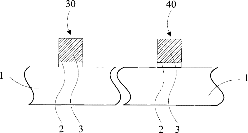
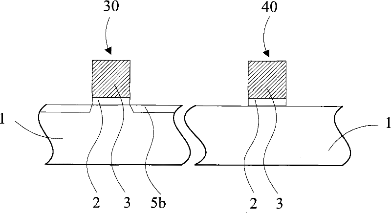
[0035] The present invention forms a fluorine ion implantation area on the surface of the semiconductor substrate above the low-doped source / drain area of ​​the n-type MOS transistor area of ​​the high voltage device area, and the fluorine ion in the fluorine ion implantation area and the silicon in the semiconductor substrate form fluorine. The silicon group prevents the formation of charge traps, prevents the accumulation of charge in the low-doped source / drain regions under voltage application, and forms a hot carrier effect.

[0036] The present invention performs rapid thermal annealing after low-doping ion implantation in the n-type MOS transistor region of the high-voltage device region. While activating impurities and eliminating defects caused by ion implantation, the TED effect and self thermal diffusion can be used to make the junction more changed. In order to gradually change, so as to further reduce the drain channel surface electric field, to achieve the purpose of ...


PUM


Abstract

The invention relates to a semiconductor device, an n-type MOS transistor and a manufacturing method thereof. The semiconductor device comprises a semiconductor substrate, a grid medium layer, a grid electrode, side walls, a light doping source / drain region, a heavy doping source / drain region, and a fluorine ion implantation region, wherein the gird medium layer, the grid electrode and the side wall are positioned inside an input / output device region of the semiconductor substrate; the low doping source / drain region and the heavy doping source / drain region are positioned inside semiconductor substrates in an n-type MOS transistor region and a p-type MOS transistor region of the input / output device region; and the fluorine ion implantation region is positioned inside a semiconductor substrate in the n-type MOS transistor region of the input / output device region. Correspondingly, the invention also provides a method for manufacturing the semiconductor device, the n-type MOS transistor and the method for manufacturing the n-type MOS transistor. The fluorine ion implantation region is formed in the low doping source / drain region of the n-type MOS transistor region, and fluorine ions inthe fluorine ion implantation region and silicon in the semiconductor substrate form fluorine-silicon groups so as to prevent the formation of charge traps, prevent the aggregation of charges in thelow doping source / drain region under the condition of additional voltage, and forming hot carrier effect.

Description

Technical field [0001] The present invention relates to the field of semiconductor technology, in particular to semiconductor devices, n-type MOS transistors and manufacturing methods thereof. Background technique [0002] As the channel length of semiconductor devices shrinks, in order to obtain the required drive current and suppress the short channel effect, a higher concentration doped semiconductor substrate and source / drain are usually used, so that the source / drain is depleted. The area generates a high electric field. When the high-voltage input / output device is operating under a saturated current state, the inversion layer charge is accelerated under the action of the lateral electric field on the channel surface and collides with the lattice to ionize, which will generate a large number of hot carriers (electron-hole pairs) . Hot electrons and hot holes can be emitted to the gate oxide layer over the interface barrier, forming a hot-carrier injection (HCI) effect. Th...

Claims


Application Information

Patent Timeline
Patent Type & Authority Patents(China)
IPC IPC(8): H01L21/8238H01L21/336H01L27/092H01L29/78H01L29/08
Inventor 赵猛王津洲
Owner SEMICONDUCTOR MANUFACTURING INTERNATIONAL (BEIJING) CORP
Why Eureka
Try Eureka