Method for flattening surface of polysilicon
A surface planarization and polysilicon technology, which is applied in the direction of electrical components, semiconductor/solid-state device manufacturing, semiconductor devices, etc., can solve the problems of reducing device reliability and service life, and achieve uniform etching rate, uniform distribution trend, polysilicon flat surface effect
- Summary
- Abstract
- Description
- Claims
- Application Information
AI Technical Summary
Problems solved by technology
Method used
Image
Examples
Embodiment 1
[0043] In the present embodiment, the operating condition of rapid thermal oxidation is: temperature is 1100 ℃, O 2 The flow rate is 8SLM (liters per minute under standard conditions), and the time for rapid thermal oxidation treatment is 3 minutes;
[0044] The power of penetration etching is 400W, the pressure is 100 mTorr, and the etching gas is CF 4 , and its flow rate is 35sccm;
[0045] The power of the main etching is 500W, the pressure is 45mTorr, and the etching gas and its flow rate are respectively 40sccmCl 2 / 60sccmHBr;
[0046] The power of over-etching is 300W, the pressure is 110mTorr, and the etching gas and its flow rate are respectively 20sccmCl 2 / 60sccmHBr / 5sccmHe-O 2 .
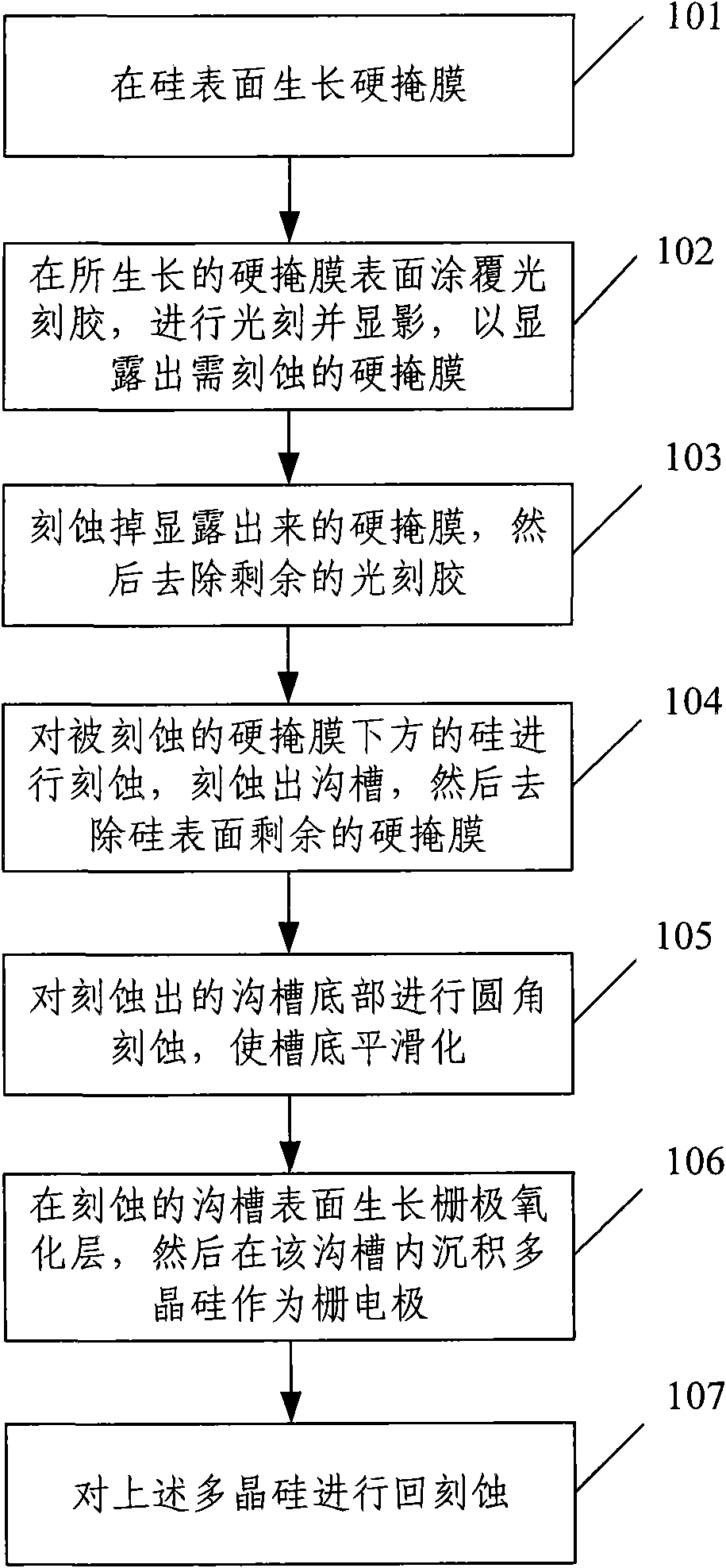
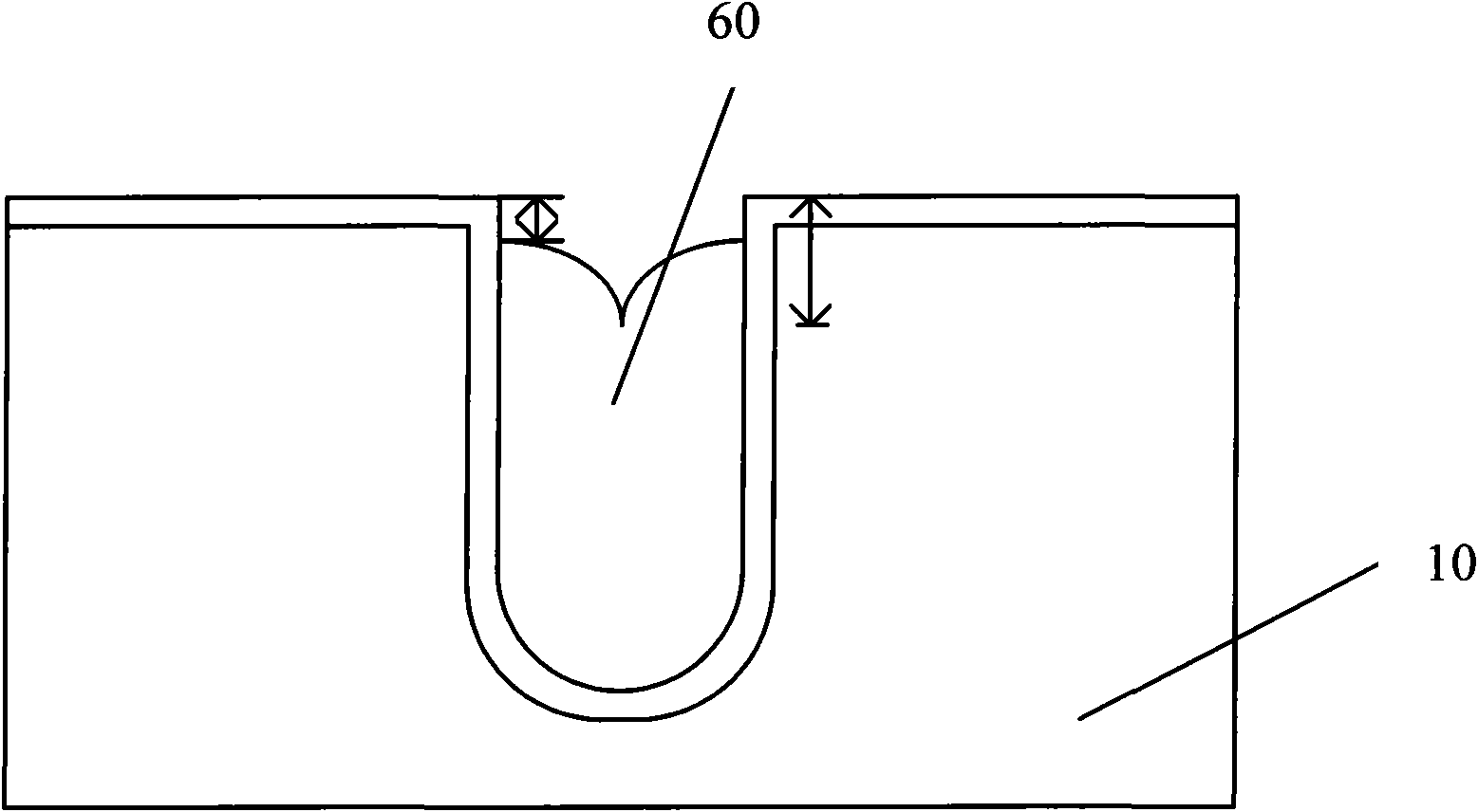
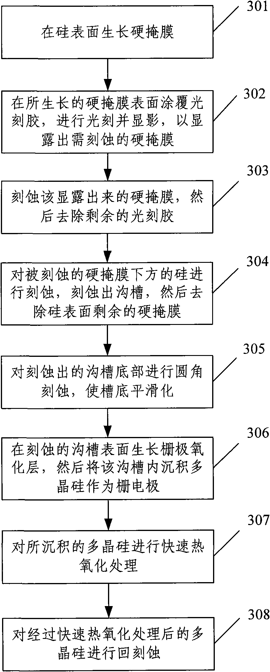
[0047] Figure 4 It is the process flow diagram of polysilicon surface planarization of the present invention, in conjunction with image 3 , Figure 4 Shown in A~4H, the method for planarizing the polysilicon surface of the present invention comprises the following steps:
[0048...
Embodiment 2
[0065] In the present embodiment, the operating condition of rapid thermal oxidation is: temperature is 900 ℃, O 2 The flow rate is 7SLM, and the time for rapid thermal oxidation treatment is 5 minutes;
[0066] The power of penetration etching is 250W, the pressure is 75 mTorr, and the etching gas is CF 4 , and its flow rate is 30 sccm;
[0067] The power of the main etching is 400W, the pressure is 40mTorr, and the etching gas and its flow rate are respectively 30sccmCl 2 / 30sccmHBr;
[0068] The power of over-etching is 250W, the pressure is 40mTorr, and the etching gas and its flow rate are respectively 30sccmCl 2 / 30sccmHBr / 8sccmHe-O 2 .
[0069] The method for planarizing the polysilicon surface of the present invention comprises the following steps:
[0070] b1) A high-temperature thermal oxide layer is grown on the surface of the single crystal silicon substrate 1, and then tetraethoxysilane is deposited on the high-temperature thermal oxide layer, and tetraethox...
Embodiment 3
[0085] In the present embodiment, the operating condition of rapid thermal oxidation is: temperature is 1100 ℃, O 2 The flow rate is 8SLM (liters per minute under standard conditions), and the time for rapid thermal oxidation treatment is 3 minutes;
[0086] The power of penetration etching is 450W, the pressure is 120mTorr, and the etching gas is CF 4 , and its flow rate is 50 sccm;
[0087] The power of the main etching is 450W, the pressure is 80mTorr, and the etching gas and its flow rate are respectively 50sccmCl 2 / 80sccmHBr;
[0088] The power of over-etching is 250W, the pressure is 120mTorr, and the etching gas and its flow rate are respectively 50sccmCl 2 / 80sccmHBr / 5sccmHe-O 2 .
[0089] The method for planarizing the polysilicon surface of the present invention comprises the following steps:
[0090] c1) Using a high temperature process to grow silicon dioxide SiO on the surface of the single crystal silicon substrate 1 2 , to serve as hard mask 2, such as ...
PUM
| Property | Measurement | Unit |
|---|---|---|
| etching power | aaaaa | aaaaa |
| etching power | aaaaa | aaaaa |
Abstract
Description
Claims
Application Information
 - R&D Engineer
- R&D Manager
- IP Professional
- Industry Leading Data Capabilities
- Powerful AI technology
- Patent DNA Extraction
Browse by: Latest US Patents, China's latest patents, Technical Efficacy Thesaurus, Application Domain, Technology Topic, Popular Technical Reports.
© 2024 PatSnap. All rights reserved.Legal|Privacy policy|Modern Slavery Act Transparency Statement|Sitemap|About US| Contact US: help@patsnap.com


