Dye-sensitized solar cell
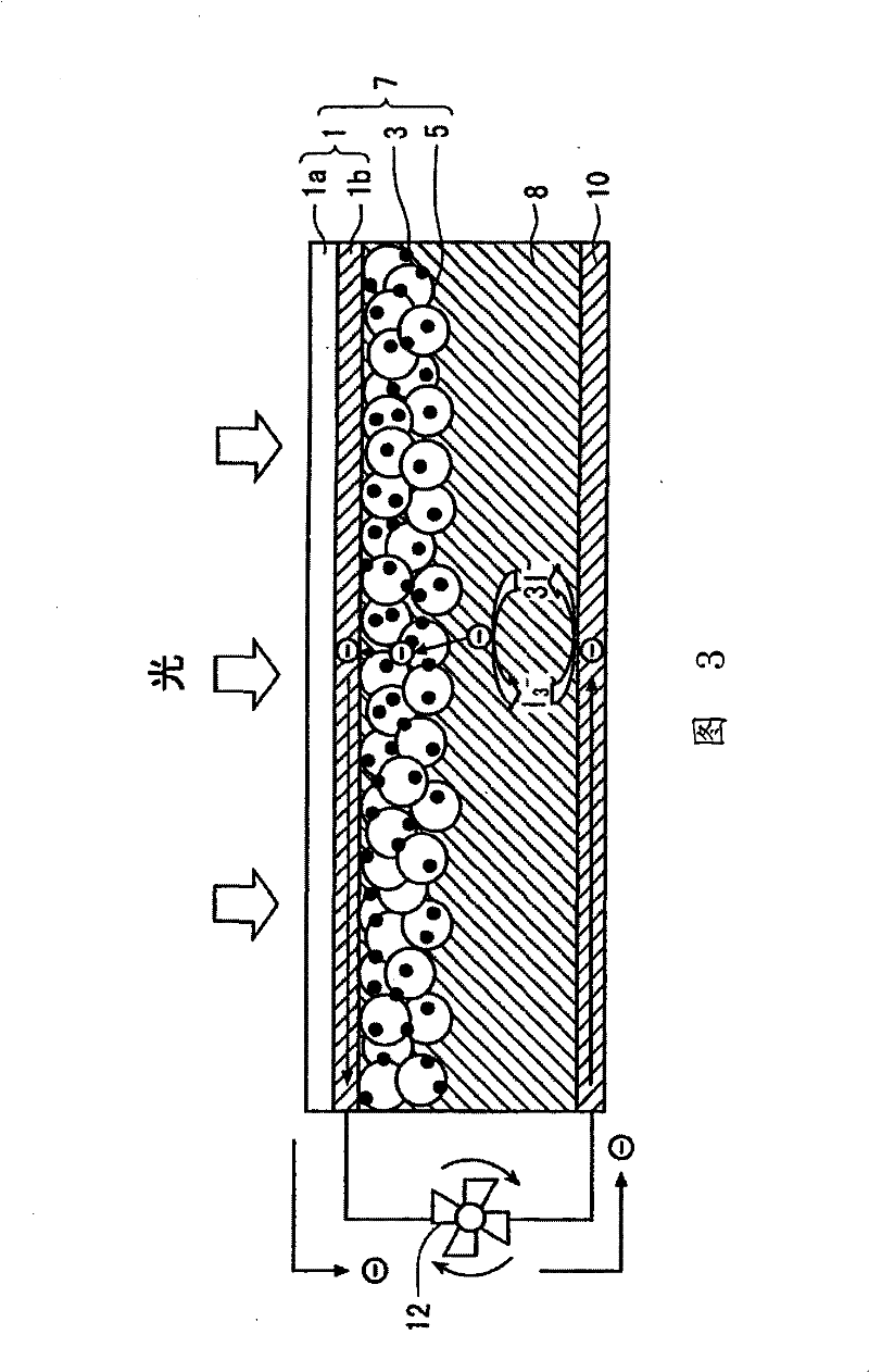
A solar cell and dye-sensitized technology, which is applied in the field of dye-sensitized solar cells, can solve the problems of reduced conversion efficiency and increased resistance of transparent conductive film 1b, and achieve the effects of avoiding reduction, avoiding conversion efficiency, and preventing corrosion
- Summary
- Abstract
- Description
- Claims
- Application Information
AI Technical Summary
Problems solved by technology
Method used
Image
Examples
Embodiment 1
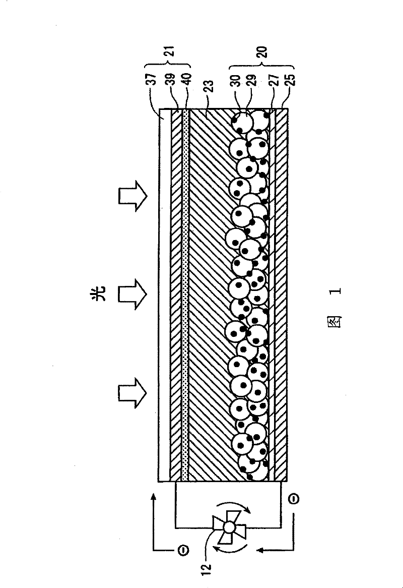
[0099] A titanium alkoxide solution was prepared by diluting with an organic solvent (butanol) so that titanium isopropoxide was 2 mol / L. A titanium dioxide microparticle paste with a solid content concentration of 20% was prepared, containing titanium dioxide particles and 20 parts by weight of the titanium alkoxide solution (general-purpose titanium dioxide particles with a particle diameter of 15 to 350 nm) based on 100 parts by weight of titanium dioxide fine particles.
[0100] In addition, the following aluminum plates treated with phosphoric acid chromate were prepared as electrode substrates.
[0101] Aluminum plate:
[0102] Thickness: 0.3mm
[0103] Chemical conversion treatment film: 50nm
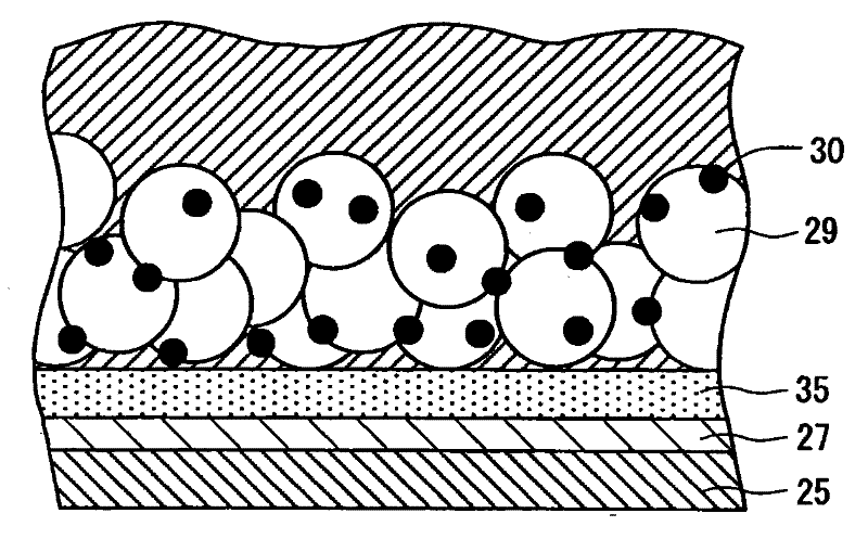
[0104] The titanium dioxide paste prepared above was applied to the chemical conversion treatment film of the aluminum plate, and fired at 450° C. for 1 hour to form an oxide semiconductor porous layer (titanium oxide layer) with a thickness of 8 μm. The surface of the titaniu...
Embodiment 2
[0121] A titanium alkoxide solution (titanium isopropoxide concentration; 2 mol / L) was prepared by diluting titanium tetraisopropoxide as a binder with an organic solvent (butanol). In addition, it was confirmed by infrared absorption spectroscopic analysis (IR) that in the titanium alkoxide solution, a part of the isopropoxy group in titanium isopropoxide was substituted with a butyl group.
[0122] Add titanium dioxide microparticles (general-purpose titanium dioxide particles with a particle diameter of 15 to 350 nm), acetylacetone (dispersant), decanol (porous accelerator) and butanol / ethanol mixed solvent (mixing ratio: 50) to the titanium alkoxide solution. / 50), a dispersion process of stirring and shaking was performed to prepare an oxide semiconductor fine particle paste. Confirmed by IR. The titanium atoms in the titanium isopropoxide in this paste form chelate bonds. The composition of the paste is as follows.
[0123] Paste composition
[0124] Solid content con...
Embodiment 3
[0136] A paste for forming an oxide semiconductor layer having a solid content concentration of 20% by weight was prepared in exactly the same manner as in Example 2 except that non-acetylacetone (dispersant) and decanol (porosity promoter) were used, and the paste was used , and in exactly the same manner as in Example 2, an 8 μm thick titanium oxide layer was formed on an aluminum plate treated with phosphoric acid chromate.
[0137] Observing the surface of the titanium oxide layer with an electron microscope, it can be seen from the photo that the formed titanium oxide layer has an area of 10000 nm per 1 μm × 1 μm area. 2 Pores with the above size accounted for 20% of the total number of pores.
[0138] A dye-sensitized solar cell was produced in the same manner as in Example 1 except that the oxide semiconductor porous layer (titanium oxide layer) was formed as described above. The conversion efficiency of the obtained battery was measured, and the measurement area was...
PUM
| Property | Measurement | Unit |
|---|---|---|
| thickness | aaaaa | aaaaa |
| thickness | aaaaa | aaaaa |
| particle diameter | aaaaa | aaaaa |
Abstract
Description
Claims
Application Information
 - R&D Engineer
- R&D Manager
- IP Professional
- Industry Leading Data Capabilities
- Powerful AI technology
- Patent DNA Extraction
Browse by: Latest US Patents, China's latest patents, Technical Efficacy Thesaurus, Application Domain, Technology Topic, Popular Technical Reports.
© 2024 PatSnap. All rights reserved.Legal|Privacy policy|Modern Slavery Act Transparency Statement|Sitemap|About US| Contact US: help@patsnap.com


