Data processing method and the device thereof
一种数据处理、数据的技术,应用在数据处理应用、电数字数据处理、数字数据处理零部件等方向,能够解决难以读取模块A等问题
- Summary
- Abstract
- Description
- Claims
- Application Information
AI Technical Summary
Problems solved by technology
Method used
Image
Examples
no. 1 example
[0256] The present embodiment is an embodiment corresponding to the first to sixth aspects of the present invention.
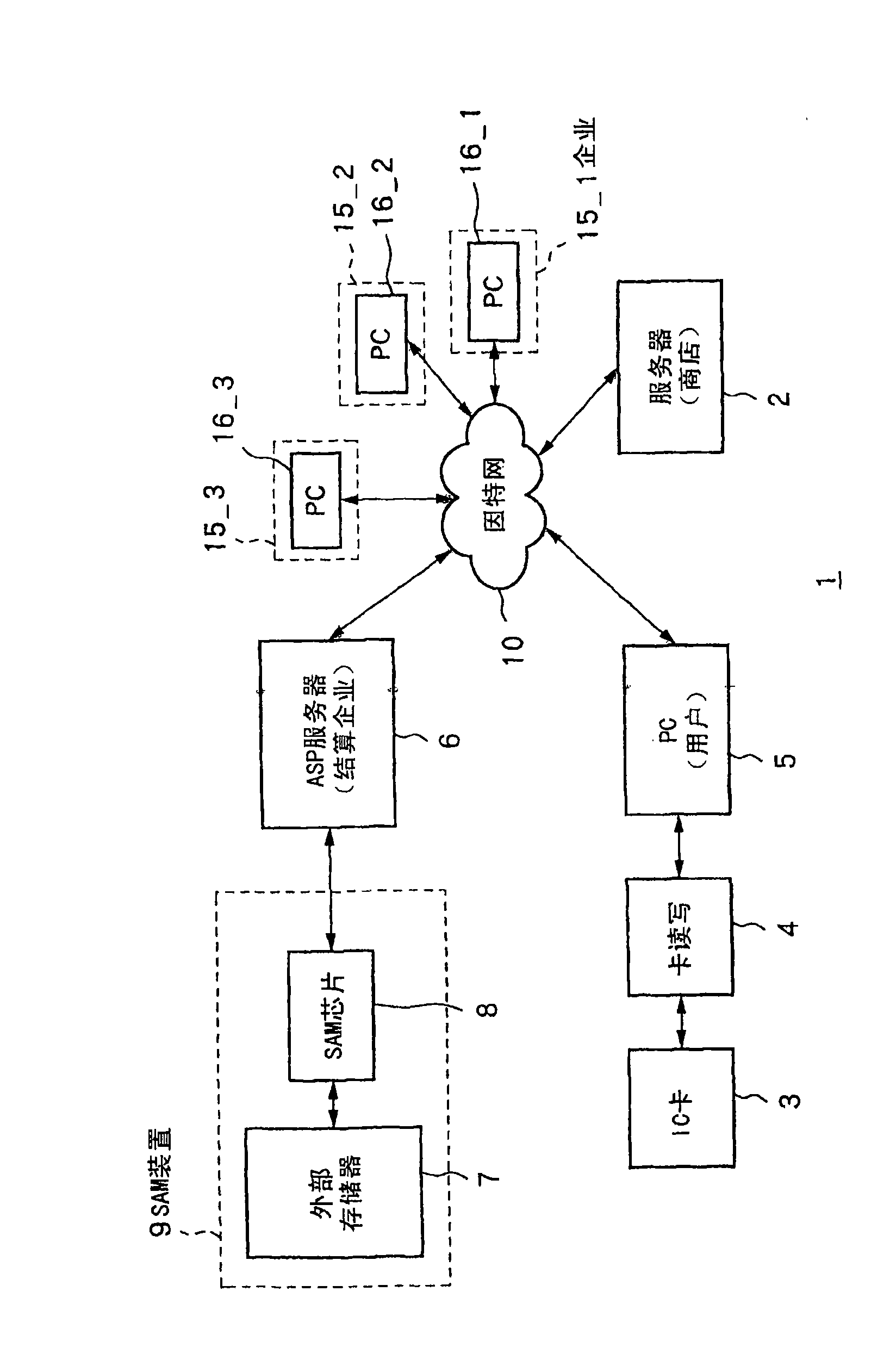
[0257] figure 1 It is the general structure of the communication system 1 of this embodiment.
[0258] Such as figure 1 As shown in , a communication system 1 communicates via the Internet 10 using a server 2, an IC card 3, a card reader / writer 4, a personal computer 5, an ASP (Application Service Provider) server 6, and a SAM (Security Application Module) device 9 , and use the IC card 3 (integrated circuit of the present invention) to complete settlement processing or other processing.
[0259] The SAM device 9 has an external memory 7 and a SAM chip (semiconductor circuit of the present invention) 8 .
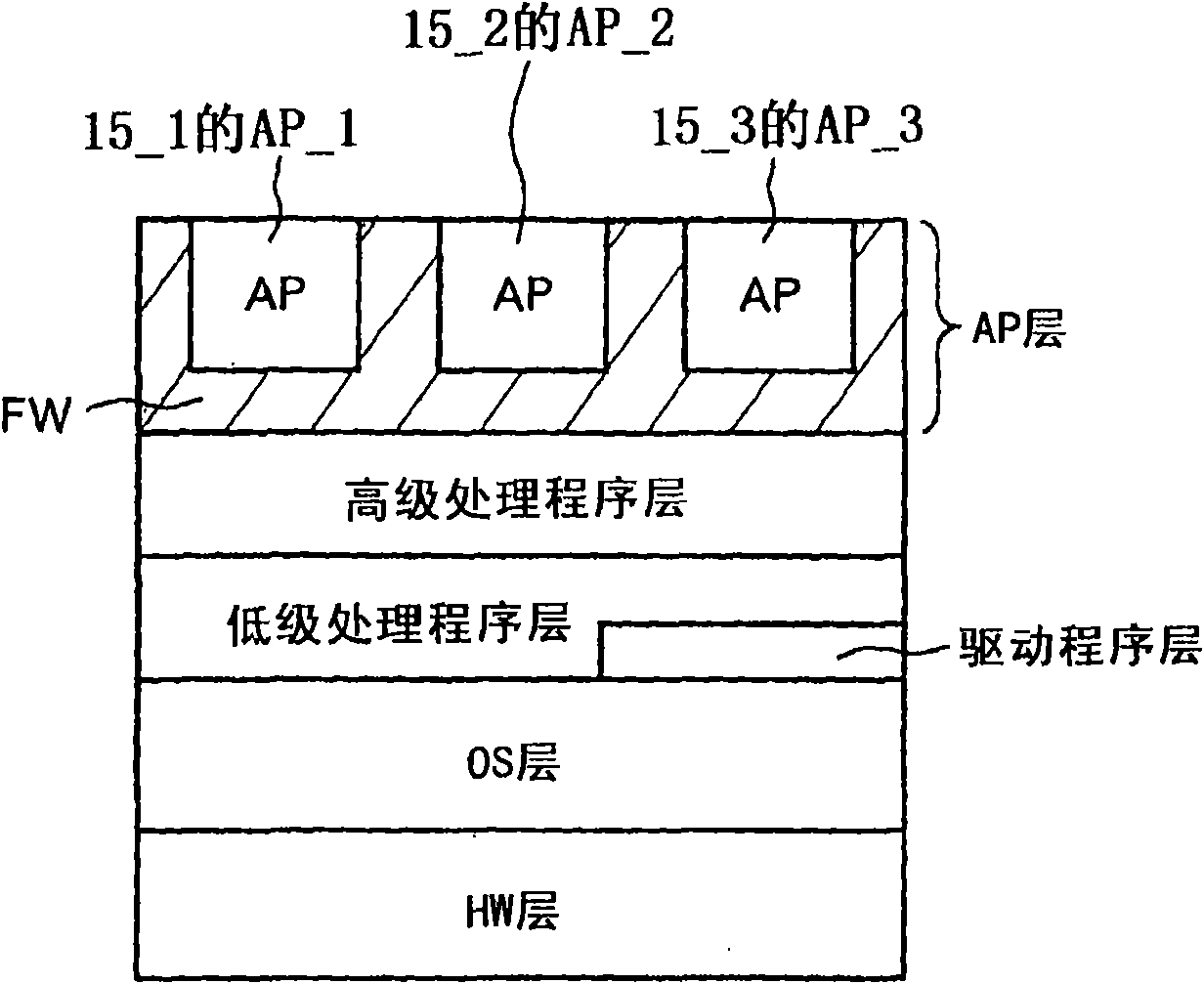
[0260] SAM chip 8 has as figure 2 The software configuration shown in .
[0261] Such as figure 2 As shown in , from the bottom layer to the top layer, the SAM chip 8 has a HW (hardware) layer, an OS layer, a low-level handler layer, a high-level h...
no. 2 example
[0467] The present embodiment is an embodiment corresponding to the seventh to ninth aspects of the present invention.
[0468] Figure 19 It is a schematic diagram of the overall structure of the communication system 101 of this embodiment.
[0469] Such as Figure 19 Shown in, communication system 101 uses server 102, IC card 103 (integrated circuit of the present invention), card reader / writer 104, personal computer 105, ASP (application service provider) server 106, SAM (security application module) ) device 109, personal computers 116_1, 116_2, and 116_3, and identity verification devices 117_1, 117_2, and 117_3 communicate through the Internet 10, and perform settlement processing or other processing of a process using the IC card 103.
[0470] The SAM device 109 has an external memory 107 (semiconductor memory circuit of the present invention) and a SAM chip 108 (semiconductor circuit of the present invention).
[0471] SAM chip 108 has Figure 20 The software confi...
no. 3 example
[0613] This embodiment is an embodiment corresponding to aspects 10-12 of the present invention.
[0614] Figure 33 The overall structure of the communication system 201 of this embodiment is shown.
[0615] Such as Figure 33 As shown in the figure, the communication system 201 uses a server 202, an IC card 203, a card reader / writer 204, a personal computer 205, an ASP (application service provider) server 206, a SAM (secure application module) device 209, and a personal computer 216_1 , 216_2, and 216_3, and identity verification devices 217_1, 217_2, and 217_3 communicate through the Internet 210, and perform settlement processing or other processing of a process using the IC card 203.
[0616] The SAM device 209 has an external memory 207 and a SAM chip 208 .
[0617] SAM chip 208 has Figure 34 The software configuration shown in .
[0618] Such as Figure 34 As shown in , from the bottom layer to the top layer, the SAM chip 208 has a HW (hardware) layer, an OS layer...
PUM
 Abstract
Description
Claims
Application Information
 - R&D
- Intellectual Property
- Life Sciences
- Materials
- Tech Scout
- Unparalleled Data Quality
- Higher Quality Content
- 60% Fewer Hallucinations
Browse by: Latest US Patents, China's latest patents, Technical Efficacy Thesaurus, Application Domain, Technology Topic, Popular Technical Reports.
© 2025 PatSnap. All rights reserved.Legal|Privacy policy|Modern Slavery Act Transparency Statement|Sitemap|About US| Contact US: help@patsnap.com


