Manufacturing method of semiconductor device

A manufacturing method, semiconductor technology, applied in semiconductor/solid-state device manufacturing, semiconductor devices, semiconductor/solid-state device components, etc., can solve the problem of inability to form aluminum sidewall protection film, difficulty in forming large pseudo-patterns, and inability to supply corrosion resistance Agent decomposition and other issues

Inactive Publication Date: 2009-08-12
SII SEMICONDUCTOR CORP
View PDF5 Cites 0 Cited by
  • Summary
  • Abstract
  • Description
  • Claims
  • Application Information

AI Technical Summary

Problems solved by technology

In addition, if the chip shrinks, the degree of freedom of the wiring layout will be narrowed, and it is expected that it will be difficult to form a large dummy pattern covered with a resist.
The portion where a large dummy pattern can be formed is located away from the wiring pattern, and there is a problem that resist decomposition products cannot contribute to the formation of the sidewall protective film
In addition, due to the influence of the micro loading effect, the resist decomposition product cannot be supplied in the fine wiring pattern, and as a result, the protective film of the aluminum side wall cannot be formed during etching, and anisotropic etching of aluminum is difficult. question

Method used


Image

  • Manufacturing method of semiconductor device
  • Manufacturing method of semiconductor device
  • Manufacturing method of semiconductor device

Examples


Embodiment Construction

[0014] Hereinafter, an embodiment of the present invention will be described based on FIGS. 1 and 2.

[0015] Fig. 1 is a process sectional view showing a first embodiment of the present invention.

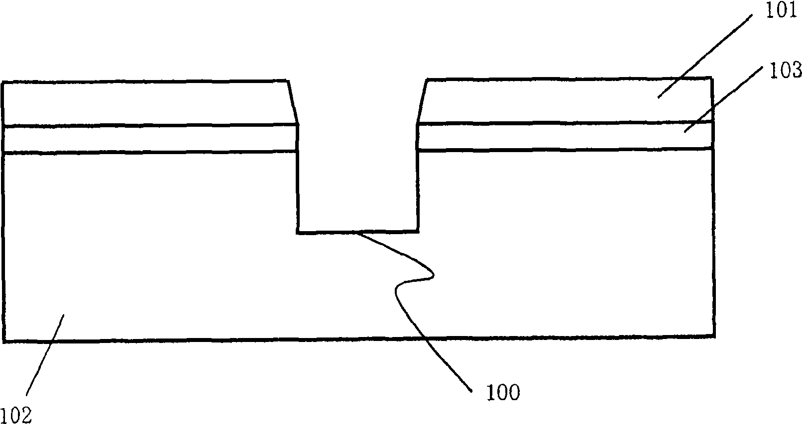
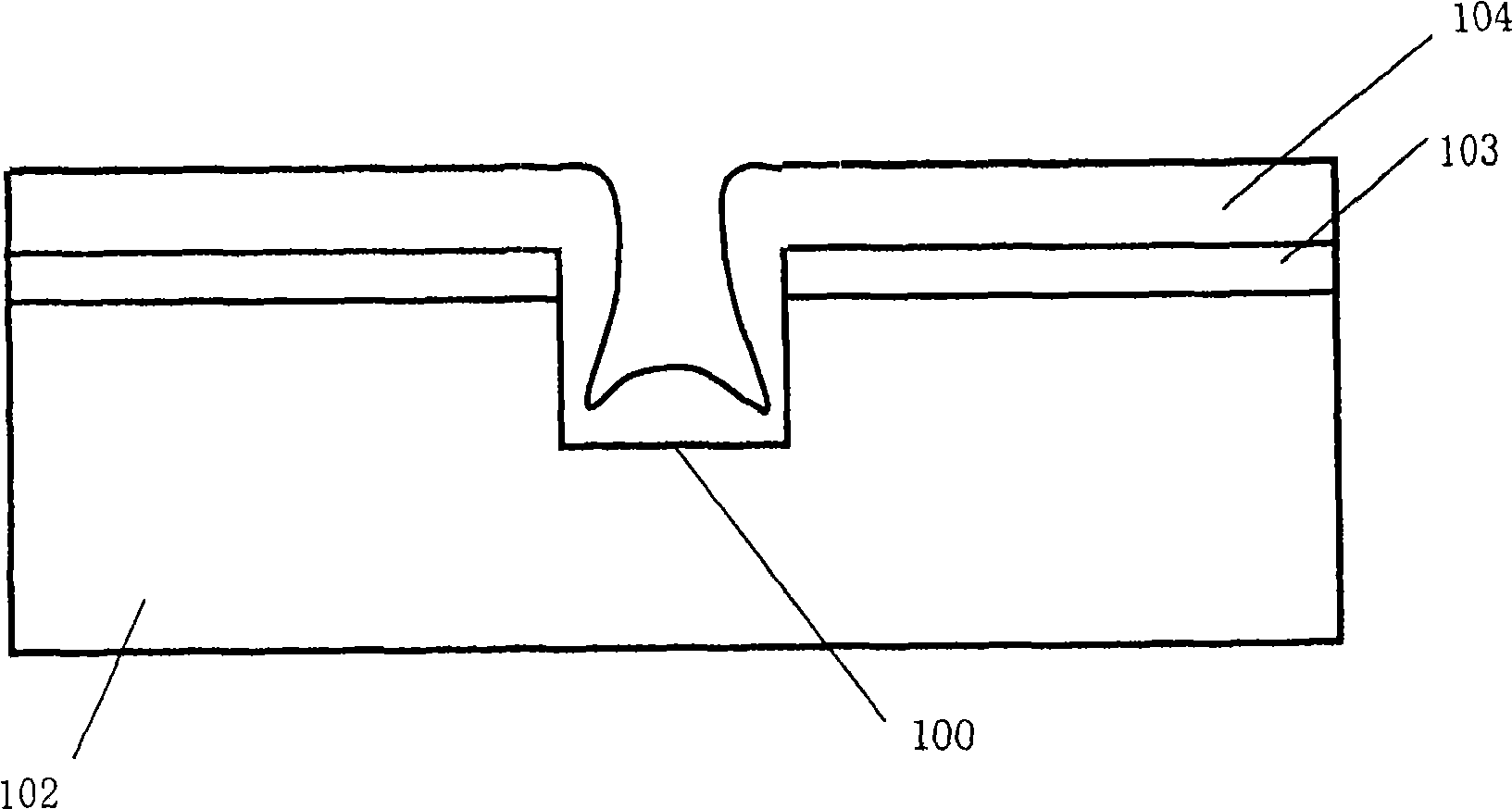
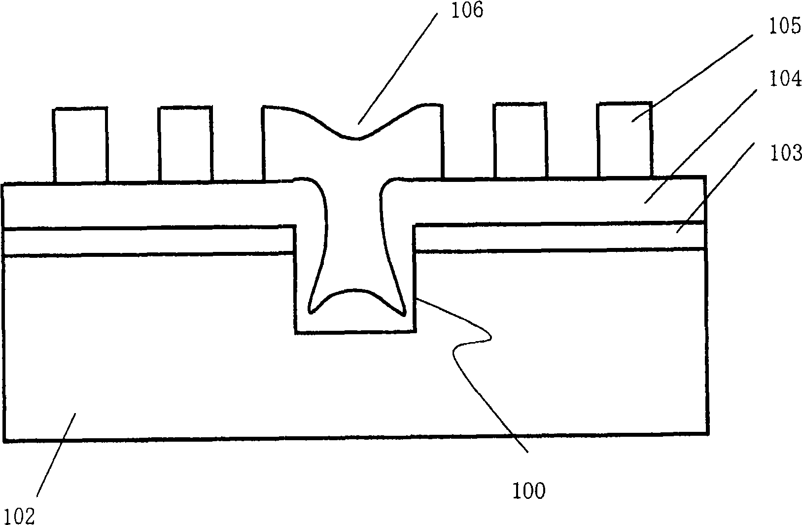
[0016] 1(A) shows a process in the middle of forming a semiconductor element on a semiconductor substrate 102, and is a cross-sectional view showing a process of forming a trench 100 after forming a contact hole of the semiconductor element. An interlayer insulating film 103 is formed on the semiconductor substrate 102, and a resist 101 is coated on the interlayer insulating film. The resist 101 is patterned, and using it as a mask, trenches 100 in the form of openings are formed in the underlying interlayer insulating film 103 and the semiconductor substrate 102 by etching. When the semiconductor element does not have a trench structure, a mask is added after forming the contact hole to form the trench 100 as in this embodiment. However, if it is a semiconductor element with a trench...


PUM


Abstract

A method of forming a metal interconnection that has a favorable cross-sectional shape is provided without the fear of side etching, even in a sparse arrangement of metal interconnections. The method, the following structure is employed. A region for placing a dummy metal interconnection is provided close to a region in which a metal interconnection is formed. A trench is formed in the dummy metal interconnection region and a resist pattern for the metal interconnection is then formed, giving the resist above the trench a large surface area per unit area. The metal interconnection is subsequently formed by dry etching in which an organic component from the resist above the trench forms a solid sidewall protection film, permitting anisotropic etching. The metal interconnection can thus have a favorable cross-sectional shape.

Description

Technical field [0001] The present invention relates to a method of manufacturing a semiconductor device, in particular to a dry etching method of metal wiring. Background technique [0002] In the dry etching process of aluminum, it is known that the resist decomposition product supplied from the resist contributes to the formation of the side wall protective film, and the side wall protective film can be used to perform anisotropic precision processing. The typical gas types for etching are Cl 2 , BCl 3 , HCl and other halogen gases. Aluminum is a metal with high reactivity, and Cl 2 The molecules react strongly, and etching proceeds at a high speed. Therefore, in order to suppress undercuts, it is necessary to form a protective film on the sidewall of the pattern. However, if the pattern is precise and the resist aperture ratio becomes high, the resist decomposition products are insufficient, the formation of the sidewall protection film is insufficient, dents occur during the...

Claims


Application Information

Patent Timeline
Patent Type & Authority Applications(China)
IPC IPC(8): H01L21/768H01L21/3213G03F7/16
CPCH01L21/32135H01L23/522H01L2924/0002H01L2924/00H01L21/306
Inventor 村田通博
Owner SII SEMICONDUCTOR CORP
Why Eureka
Try Eureka