Load bearing belt for packing chip and chip packaging structure

A chip packaging structure and carrier tape technology, applied in electrical components, electrical solid-state devices, circuits, etc., can solve problems such as poor production and testing efficiency, large process time, and carrier tape waste.

Active Publication Date: 2009-07-01
CHIPMOS TECH INC
View PDF0 Cites 6 Cited by
  • Summary
  • Abstract
  • Description
  • Claims
  • Application Information

AI Technical Summary

Problems solved by technology

Conceivably, if the area used by the first test pad area 13 and the second test pad area 13' is larger, the parts to be cut and removed will be more, which will cause unnecessary waste of the carrier tape 10
In addition, in the existing chip packaging structure 1, when performing an electrical test on the chip 21, the probes of the electrical testing device are sequentially and repeatedly electrically connected to the test pad 131 and the test pad 131', This electrical test needs to move the probe repeatedly, resulting in a lot of process time, making the production test efficiency not good

Method used


Image

  • Load bearing belt for packing chip and chip packaging structure
  • Load bearing belt for packing chip and chip packaging structure
  • Load bearing belt for packing chip and chip packaging structure

Examples


Embodiment Construction

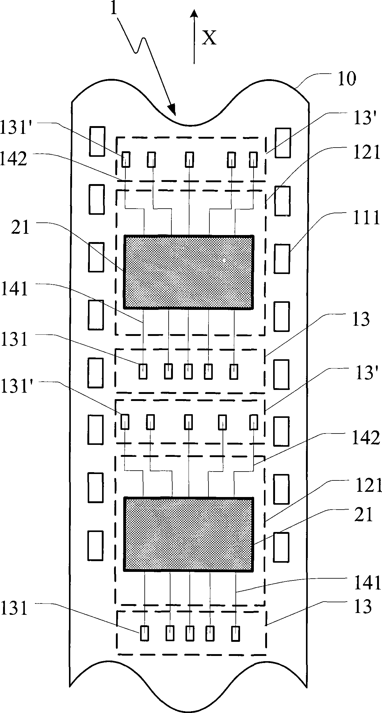
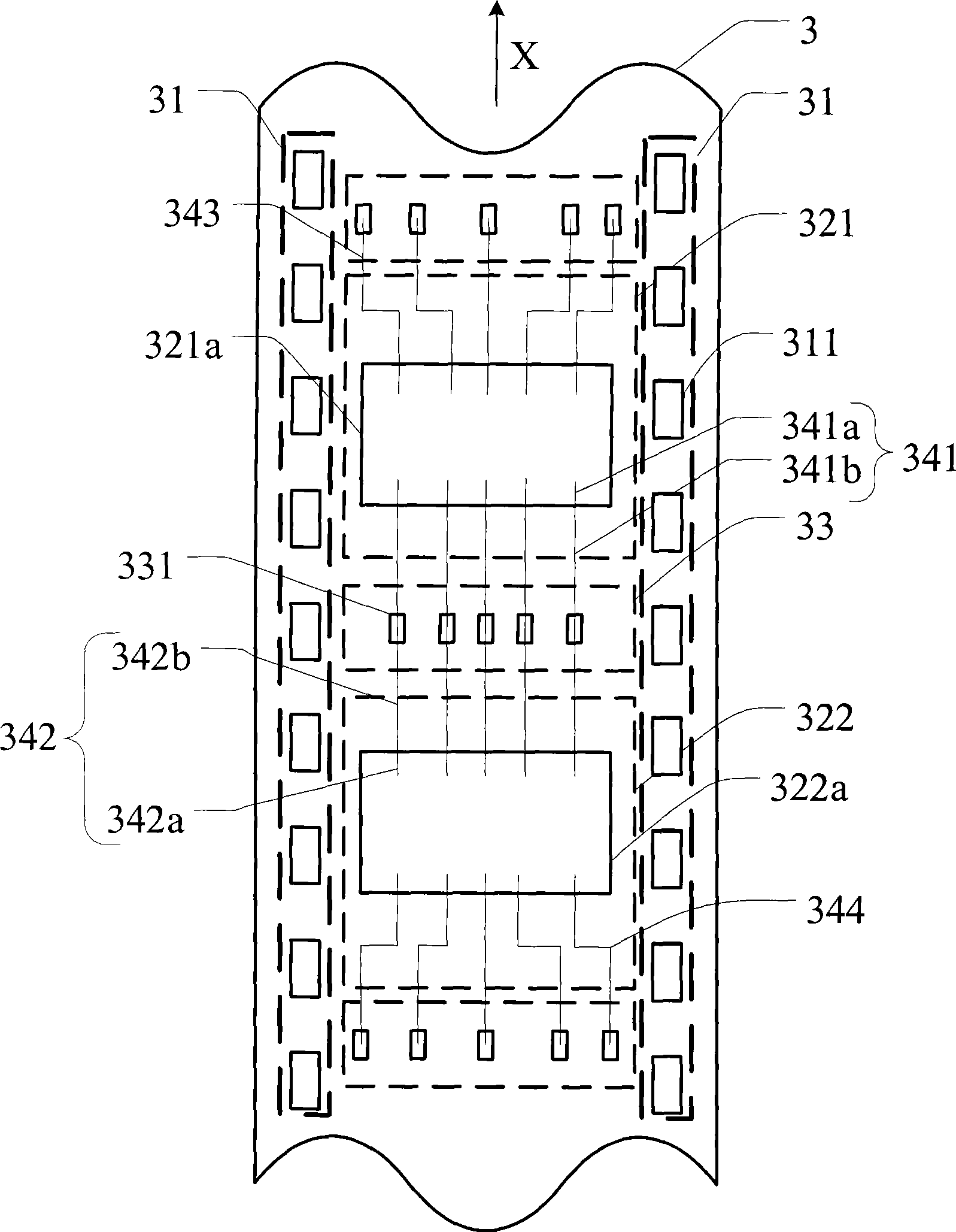
[0034] An embodiment of the present invention discloses a carrier tape 3 for packaging chips, which can extend along a conveying direction X, such as figure 2 As shown, the carrier strip 3 at least includes two transmission areas 31 , two packaging areas 321 and 322 , a test pad area 33 , a plurality of test pads 331 disposed on the test pad area 33 and a metal circuit layer.

[0035] In this embodiment, the two transmission areas 31 of the carrier belt 3 are respectively defined on the two sides of the carrier belt 3 and extend along the conveying direction X. , and adjacent to a plurality of positioning holes 311 disposed on two sides of the carrier belt 3 . The carrier tape 3 is transported and positioned through the positioning hole 311. For example, when the carrier tape 3 is positioned at one position, it is suitable for chip packaging, and then positioned at another position for cutting.

[0036] For convenience of description, the encapsulation areas 321 and 322 can ...


PUM


Abstract

The invention relates to a bearing strip used for packing chips and a chip packing structure, wherein a plurality of sharing testing pads are arranged in a testing pad area of two packing areas on the bearing strip, which are simultaneously electrically connected with the two packing areas, which reduces the area of the testing pad on the bearing strip, reduces cutting waste, and can save repeated acting time of electrical testing devices in electrical testing, thereby improving testing efficiency.

Description

technical field [0001] The invention relates to a carrier tape and a chip packaging structure for packaging chips; in particular, a carrier tape and a chip packaging structure with a common test pad area. Background technique [0002] With the advancement of industry, various liquid crystal screens and electronic products with folding functions have been widely used in daily life. Among them, because the flexible circuit board has the advantages of thin thickness, small pin spacing, and high number of pins, when the LCD screen is to save space, or the electronic product is to achieve the function of folding, the flexible circuit board becomes indispensable. missing components. [0003] Generally speaking, the flexible circuit board utilizes chip packaging technology to bond semiconductor chips thereon. Among them, the Tape Automatic Bonding (TAB) technology is to fix the chip on the carrier tape, and use the bumps or pads of the chip to align with the metal lead layer of t...

Claims


Application Information

Patent Timeline
IPC IPC(8): H01L23/498H01L23/544
Inventor 沈弘哲
Owner CHIPMOS TECH INC
Why Eureka
Try Eureka