Method for dry method etching polycrystalline silicon in deep plow groove

A dry etching, polysilicon technology, used in electrical components, semiconductor/solid-state device manufacturing, circuits, etc., can solve problems such as excessive polysilicon gaps and increased polysilicon surface roughness, to eliminate gap expansion and reduce etching. amount of effect

Active Publication Date: 2009-05-20
SHANGHAI HUAHONG GRACE SEMICON MFG CORP
View PDF0 Cites 8 Cited by
  • Summary
  • Abstract
  • Description
  • Claims
  • Application Information

AI Technical Summary

Problems solved by technology

[0003] The technical problem to be solved by the present invention is to provide a method for dry etching polysilicon in deep trenches, which can prevent the problems of excessive polysilicon gaps and increased surface roughness of polysilicon, thereby achieving the purpose of improving device performance

Method used


Image

  • Method for dry method etching polycrystalline silicon in deep plow groove
  • Method for dry method etching polycrystalline silicon in deep plow groove
  • Method for dry method etching polycrystalline silicon in deep plow groove

Examples


Embodiment Construction

[0013] In the manufacturing process of the power MOS device, in order to form a double-layer polysilicon gate structure in the deep trench, in one embodiment of the present invention, the following method can be used:

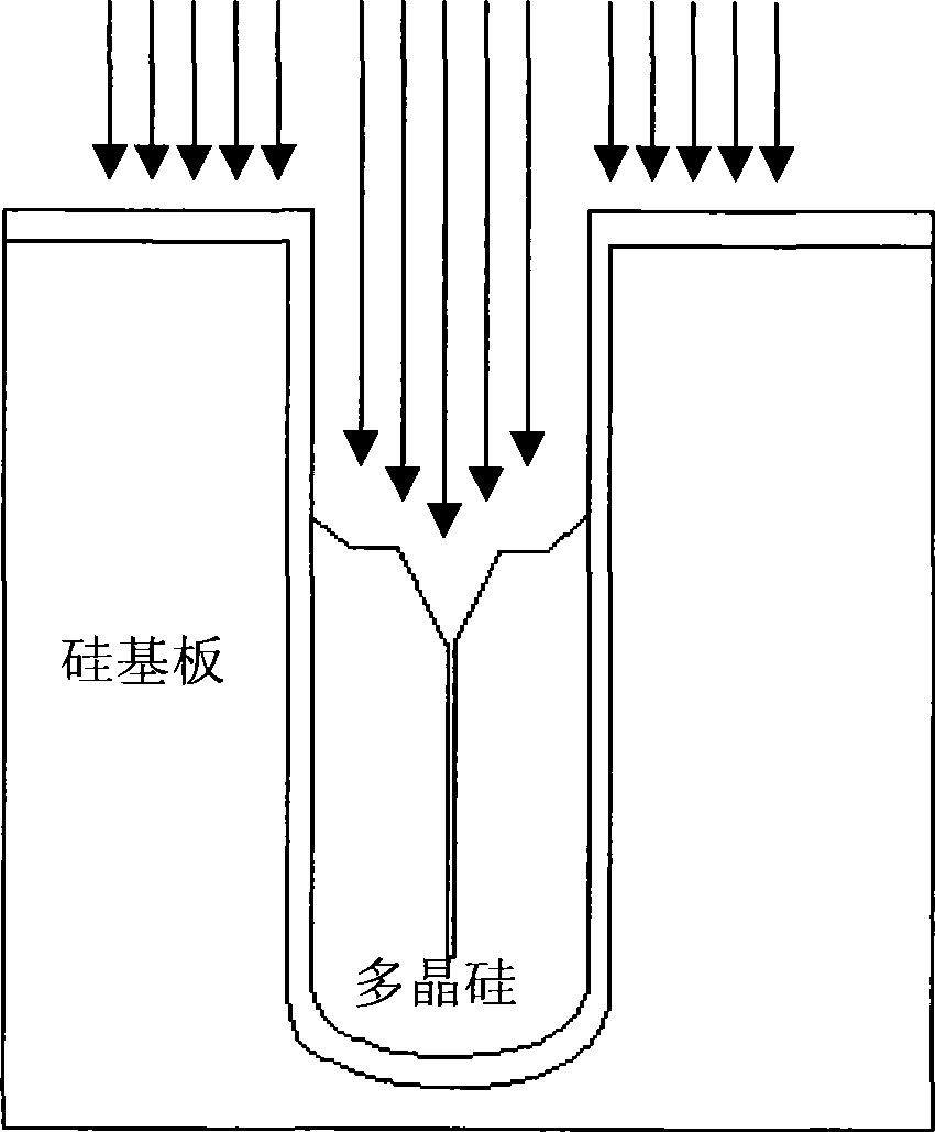
[0014] In the first step, using existing processes, a layer of Thick polysilicon to fill up the deep trench, then the structure diagram of the device is as follows figure 1 shown.

[0015] The second step is to use chlorine, hydrogen bromide and oxygen, and perform the first dry etching on the polysilicon deposited in the deep trench with a lower power of 20-200W, so as to remove the polysilicon on the surface and part of the trench polysilicon, then the structure diagram of the device is as follows figure 2 shown.

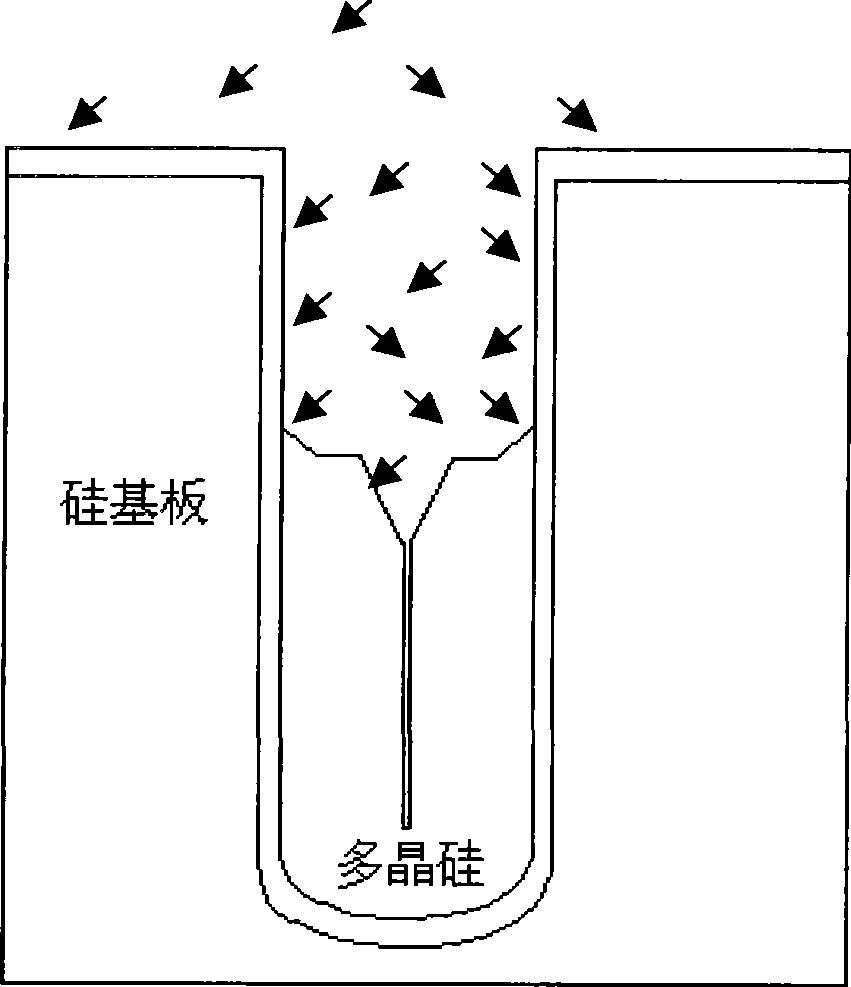
[0016] The third step, as mentioned above, due to the above-mentioned first dry etching, the polysilicon has the disadvantages of larger gaps and higher surface roughness, so in the present invention, as image 3 shown, and then carbon tetraf...


PUM


Abstract

The invention discloses a method for dry etching for polycrystalline silicon in a deep groove, which comprises the following steps: after the dry etching for the polycrystalline silicon deposited in the deep groove by larger lower power through using chlorine, hydrogen bromide and oxygen, using carbon tetrafluoride and the chlorine as main etching gases, and using lower bias power to etch the polycrystalline silicon again approximately to each isotropic property to reduce etching amount in the vertical direction, thereby solving the problem of gap expansion, and obtaining a flat polycrystalline silicon surface simultaneously.

Description

technical field [0001] The invention relates to the field of manufacturing power MOS devices in integrated circuits, in particular to a method for dry etching polysilicon in deep trenches when forming a double-layer polysilicon gate structure. Background technique [0002] In the manufacturing process of power MOS devices, it is necessary to form a double-layer polysilicon gate structure in the deep trench. The specific formation method of the gate structure described in the prior art includes the following steps: (1) in the deep trench deposit a layer thick polysilicon to fill the deep trenches, however, due to limitations in polysilicon growth methods, such as figure 1 As shown, there will be another gap in the polysilicon deposited in the deep trench. (2) Use chlorine gas, hydrogen bromide and oxygen, and carry out dry etching method to the polysilicon deposited in the deep trench with a relatively large lower power, to remove the polysilicon on the surface and a part ...

Claims


Application Information

Patent Timeline
Patent Type & Authority Applications(China)
IPC IPC(8): H01L21/3065H01L21/28C23F4/00
Inventor 吉黎虞颖李虹王一张开敏
Owner SHANGHAI HUAHONG GRACE SEMICON MFG CORP
Why Eureka
Try Eureka