Method of forming wiring pattern and method of manufacturing TFT substrate using the same

a thin film transistor and wiring pattern technology, applied in the direction of cable/conductor manufacturing, decorative surface effects, decorative arts, etc., can solve the problems of difficult application of etching resist technology to tft substrate, increase manufacturing cost, etc., to achieve shortened manufacturing lead time for tft substrate, reduced amount of etching resist used, and improved manufacturing efficiency

Inactive Publication Date: 2010-05-18
NEC LCD TECH CORP
View PDF14 Cites 2 Cited by
  • Summary
  • Abstract
  • Description
  • Claims
  • Application Information

AI Technical Summary

Benefits of technology

[0027]In the method of forming a wiring pattern of the present invention, in the case where an upper wiring which interests with a lower wiring pattern is formed, an etching resist pattern is formed by screen printing and, thereafter, softened. This softening of the pattern enables repair of defects such as spaces which are formed on a step part of a conductive film for the upper wiring, the step part being formed due to the lower wiring pattern, and which are generated in the etching resist pattern. As a result, it is possible to prevent occurrence of defects such as disconnection and a wiring defect of a portion of the upper wiring which intersects with the lower wiring.
[0029]In the method of manufacturing a TFT substrate of the present invention, by adopting the above-described method of forming a wiring pattern of the present invention, an amount of the etching resist used can be reduced, and manufacturing lead-time for the TFT substrate can also be shortened. In the present invention, the upper wiring can be formed by screen printing using a conductive paste as a wiring material. Thus, the manufacturing lead time for the TFT substrate can be further shortened.

Problems solved by technology

As a result, the photoresist formation process is a cause of an increase of the manufacturing cost.
However, the technologies described above can only be applied to a relatively large pattern.
For example, it has been difficult to apply the technologies to a TFT substrate which enables high-definition display such as that demanded in market.
Thus, a wiring defect or disconnection occurs.

Method used


Image

  • Method of forming wiring pattern and method of manufacturing TFT substrate using the same
  • Method of forming wiring pattern and method of manufacturing TFT substrate using the same
  • Method of forming wiring pattern and method of manufacturing TFT substrate using the same

Examples


embodiment 1

Typical Embodiment 1

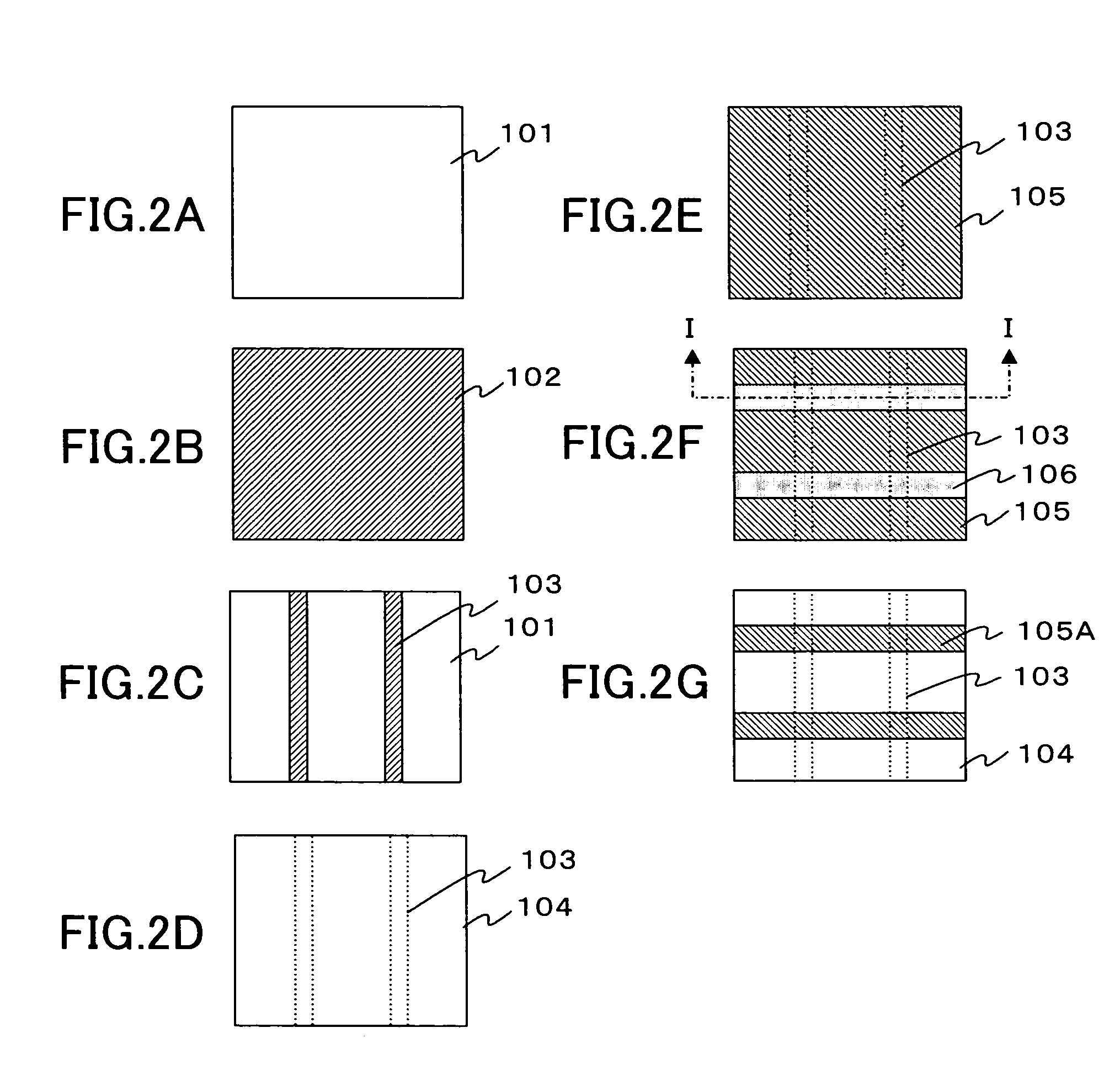
[0043]FIGS. 2A to 2F are plan views of a main part of a substrate, showing steps of a method of forming a wiring according to a first typical embodiment of the present invention. First, as shown in FIG. 2A, an insulating substrate 101 such as a glass substrate is prepared. Next, as shown in FIG. 2B, a first wiring metal film 102 is deposited on the entire surface of the insulating substrate 101. As the first wiring metal film 102, a laminated film can be used, which is formed of one selected from a group including Cr, Ta, Mo and Ti, and an aluminum alloy film such as Al—Nd and Al—Ta.

The first wiring metal film 102 has a thickness of 200 nm to 1000 nm.

[0044]Next, as shown in FIG. 2C, an unnecessary portion of the wiring metal film 102 is etched by wet etching or dry etching using a resist as a mask, and a first wiring pattern 103 is formed. Next, as shown in FIG. 2D, an insulating film 104 having a thickness of 200 to 1000 nm is deposited on the entire surface of ...

embodiment 2

Typical Embodiment 2

[0049]Next, with reference to FIGS. 4A to 4F, description will be given of a method of forming a wiring according to a second typical embodiment of the present invention. First, as shown in FIG. 4A, an insulating substrate 601 such as a glass substrate is prepared. Next, as shown in FIG. 4B, a wiring metal film 602 is deposited on the entire surface of the insulating substrate 601. As the wiring metal film 602, a laminated film can be used, which is formed of one selected from a group including Cr, Ta, Mo and Ti, and an aluminum alloy film such as Al—Nd and Al—Ta. The wiring metal film 602 has a thickness of 200 nm to 1000 nm. Next, as shown in FIG. 4C, an unnecessary portion of the wiring metal film 602 is etched by wet etching or dry etching using a resist as a mask. Thus, a first wiring pattern 603 is formed. Note that the first wiring pattern 603 may be formed by using a screen printing method to directly print a conductive resin onto the insulating substrate...

embodiment 3

Typical Embodiment 3

[0053]With reference to FIGS. 5A to 6J, description will be given of a method of manufacturing a TFT substrate according to a third typical embodiment of the present invention. First, as shown in FIG. 5A, a gate wiring film 302 is deposited on an insulating substrate 301 such as a glass substrate. As the gate wiring film 302, a laminated film can be used, which is formed of one selected from a group including Cr, Ta, Mo and Ti, and an aluminum alloy film such as Al—Nd and Al—Ta. Next, as shown in FIG. 5B, a resist pattern 303 having a thickness of 2 to 5 μm is formed by use of a screen printing method. By using the resist pattern 303 as a mask, as shown in FIG. 5C, the gate wiring film 302 is etched to pattern a gate wiring 302A. Thereafter, as shown in FIG. 5D, the resist pattern 303 on the gate wiring 302A is removed. Next, as shown in FIG. 5E, a gate insulating film 304 and a semiconductor film 305 are sequentially deposited on the insulating substrate 301 hav...


PUM

PropertyMeasurementUnit
temperatureaaaaaaaaaa
timeaaaaaaaaaa
thicknessaaaaaaaaaa

Abstract

A method of forming a wiring pattern includes forming a first conductive film pattern, an insulating film and a second conductive film pattern intersecting with the first conductive film pattern on an insulating substrate. In the method, an etching resist pattern for forming the second conductive film pattern is formed by use of a screen printing method. Thereafter, an etching resist is softened by exposing the etching resist in an organic solvent atmosphere before hardening thereof. Thus, defects such as spaces in the etching resist are repaired. By use of the above-described method of forming a wiring pattern, a TFT substrate is manufactured.

Description

BACKGROUND OF THE INVENTION[0001]1. Field of the Invention[0002]The present invention relates to a method of forming a wiring pattern and a method of manufacturing a thin film transistor (TFT) substrate using the same. More particularly, the present invention relates to a method of forming a wiring pattern by use of a screen printing method, and a method of manufacturing a TFT substrate using the same.[0003]2. Description of the Related Art[0004]In a color liquid crystal display panel of a color liquid crystal display, manufacturing of a high-definition panel has been underway. For manufacturing of the high-definition panel, conventionally, there has been adopted a method of narrowing a pitch between pixels of a color filter and a thin film transistor (TFT) and reducing a line width of a black matrix (BM) of the color filter and line widths of a data line and a gate line of the TFT.[0005]Moreover, in manufacturing of the color liquid crystal display panel, manufacturing of a TFT sub...

Claims


Application Information

Patent Timeline
Patent Type & Authority Patents(United States)
IPC IPC(8): G03F7/26
CPCH01L29/66765G02F1/136286G02F2001/13629H01L27/1292H01L27/124G02F1/13629G02F1/136
Inventor YAMAMOTO, YUJI
Owner NEC LCD TECH CORP
Why Eureka
Try Eureka