
Infrared-ultraviolet multi-color detector and production process thereof

A detector and ultraviolet technology, applied in semiconductor devices, final product manufacturing, sustainable manufacturing/processing, etc., can solve problems such as unfavorable system integration, complex packaging, high cost, etc., to enhance recognition ability, reduce false alarm rate, cost high effect

Active Publication Date: 2009-04-29
THE 13TH RES INST OF CHINA ELECTRONICS TECH GRP CORP
View PDF0 Cites 20 Cited by
  • Summary
  • Abstract
  • Description
  • Claims
  • Application Information

AI Technical Summary

Problems solved by technology

The current common technical solution is generally to simply combine independent infrared band detectors and ultraviolet band detectors to form an infrared / ultraviolet multicolor detector, but its packaging is complicated, large in size and high in cost, which is not conducive to system integration
In recent years, a GaN / AlGaN monolithic integrated infrared / ultraviolet detector structure based on the idea of ​​HEIWIP has been reported abroad. However, due to its design, the n+GaN emitter is located on the light incident side, and its Al composition is lower than that of AlGaN. The barrier region causes the ultraviolet radiation absorbed by the barrier region to be greatly reduced, so its ultraviolet response is very low
If this emitter layer is etched away, the infrared response will be reduced by four times, while the ultraviolet response will only be increased by two times. and infrared applications

Method used


Image

  • Infrared-ultraviolet multi-color detector and production process thereof
  • Infrared-ultraviolet multi-color detector and production process thereof
  • Infrared-ultraviolet multi-color detector and production process thereof

Examples


Embodiment Construction

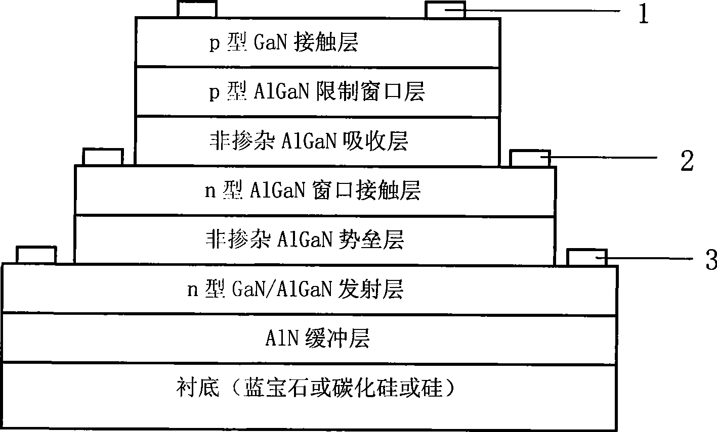
[0019] Such as figure 1 As shown, the infrared-ultraviolet multicolor detector grows AlN buffer layer, n-type GaN / AlGaN emission layer, non-doped AlGaN barrier layer, n-type AlGaN window contact layer, non-doped AlGaN absorption layer on the substrate sequentially. Layer, p-type AlGaN confining window layer and p-type GaN contact layer form a two-level convex multi-color detector mesa, with n-type GaN / AlGaN emitter layer and n-type AlGaN window contact layer as protrusions. There is an n-type lower contact electrode 3 on the boss of the n-type GaN / AlGaN emitter layer, an n-type middle contact electrode 2 on the boss of the n-type AlGaN window contact layer, and a p-type upper contact electrode on the p-type GaN contact layer. Contact electrode 1.

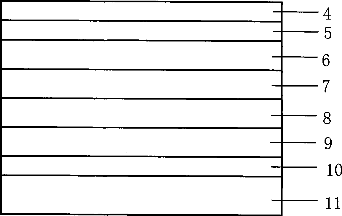
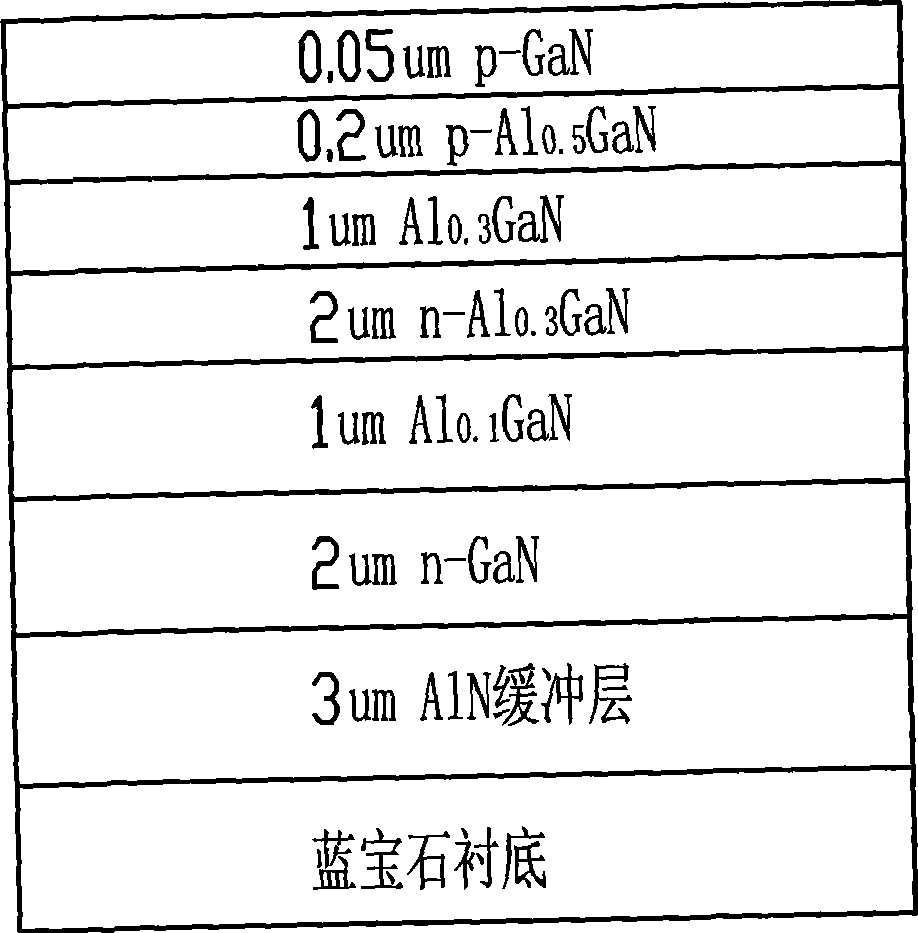
[0020] The substrate described in this infrared-ultraviolet multicolor detector is preferably Si, sapphire or silicon carbide polished substrate, in order to achieve better infrared / ultraviolet detection effect, such as figure 2 ...


PUM


Abstract

The invention discloses an infrared-ultraviolet multicolor detector and a preparation method thereof. The detector comprises a substrate, a multicolor detector table which is formed by orderly growing an AlN buffer layer, an n-type GaN / AlGaN emission layer, an undoped AlGaN barrier layer, an n-type AlGaN window contact layer, an undoped AlGaN absorbing layer, a p-type AlGaN limiting window layer and a p-type GaN contact layer on the substrate; an n-type bottom contact electrode is arranged on the n-type GaN / AlGaN emission layer, an n-type intermediate contact electrode is arranged on the n-type AlGaN window contact layer, and a p-type top contact electrode is arranged on the p-type GaN contact layer. The detector has the advantages of simple structure, easy growth, small volume, being capable of realizing triband response and the like. The detector simplifies the growth process and the processing technology of the device structure, improves the radioresistance capacity of the device, reduces the device volume and lowers the cost. The detector has significant application prospects in the fields of target imaging, alarming, monitoring and the like.

Description

technical field [0001] The invention belongs to the technical field of photodetectors, in particular to an infrared-ultraviolet multicolor detector and a preparation method thereof. Background technique [0002] All objects emit thermal radiation related to their temperature and properties, with most of the thermal radiation from objects near ambient temperature in the infrared band. Infrared radiation occupies a fairly wide electromagnetic wave band (0.8 μm ~ 1000 μm). It can be seen that infrared radiation provides rich information of the objective world, and making full use of this information is the goal pursued by people. At present, the detection technology of infrared radiation is very mature, and it is widely used in military and civilian applications, such as infrared imaging, infrared early warning, infrared monitoring, etc. In contrast, the false alarm rate of ultraviolet radiation detection is much lower, but the detection distance is shorter. In recent years,...

Claims


Application Information

Patent Timeline
IPC IPC(8): H01L31/101H01L31/18
CPCY02P70/50
Inventor 尹顺政李献杰蔡道民齐利芳赵永林
Owner THE 13TH RES INST OF CHINA ELECTRONICS TECH GRP CORP
Learn More