
Method for making flash memory

A memory and flash technology, applied in the field of flash memory production, can solve problems such as uneconomical, low adhesion of metal silicide layer 22, abnormal oxidation, etc., and achieve improved silicon/tungsten distribution ratio and improved word line sheet resistance. Problems, the effect of avoiding abnormal oxidation

Inactive Publication Date: 2009-04-01
POWERCHIP SEMICON CORP
View PDF0 Cites 18 Cited by
  • Summary
  • Abstract
  • Description
  • Claims
  • Application Information

AI Technical Summary

Problems solved by technology

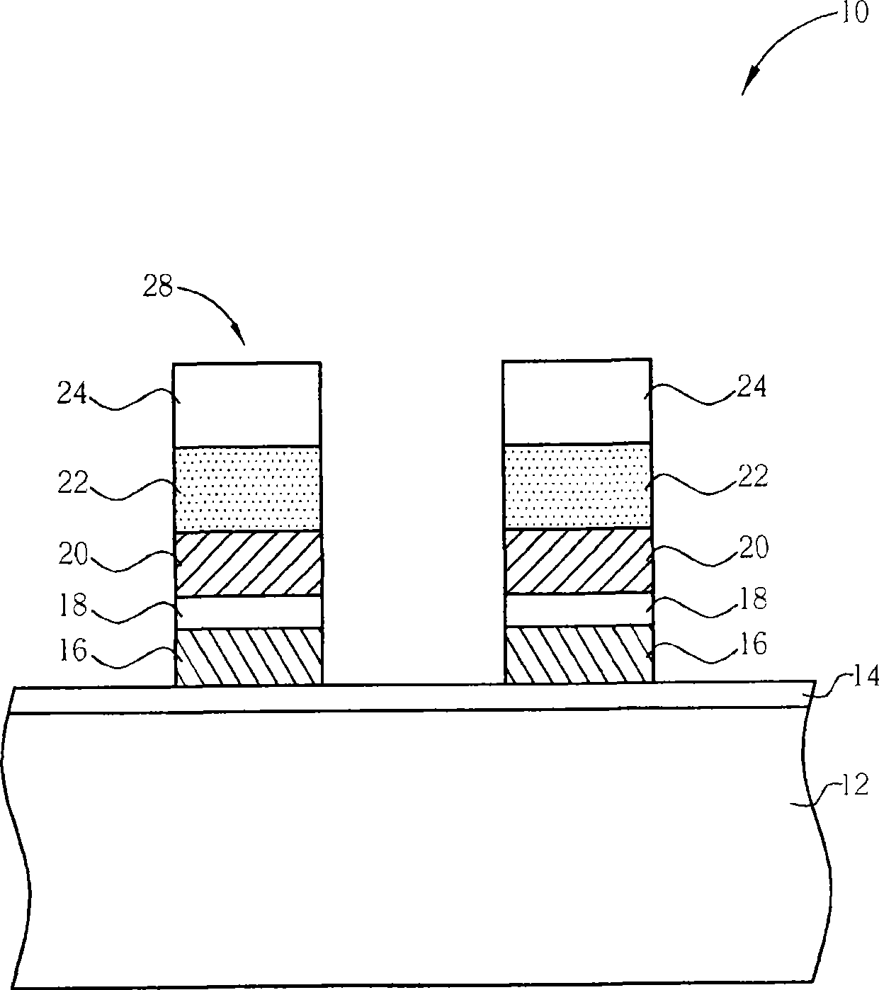
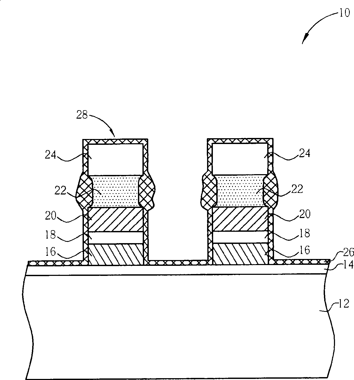
However, if figure 2 As shown, an improper thermal process will eat part of the metal silicide layer 22 inwardly, and cause abnormal oxidation on the sidewall of the stacked structure 28, for example, the oxide layer 26 on the sidewall surface of the metal silicide layer 22 has a relatively high large thickness
In this case, if the thickness of the metal silicide layer 22 is too thick, or the integration degree of the memory cell is relatively large, that is, when the aspect ratio (aspect ratio) is relatively large, the oxide layer 26 produced by the thermal process may be too large. It is thick and has an irregular shape, so that voids (voids) are generated between adjacent stacked structures 28, causing the material in the subsequent process to be unable to effectively fill the area between the stacked structures 28, and water vapor infiltrates into the voids to affect the separation grid. Extreme Flash Memory 10 Reliability
In addition, the adhesiveness of the metal silicide layer 22 will be lower after the thermal process, causing the possibility of word line peeling off.
[0006] It can be seen from the above that although the known technology attempts to improve the problem of word line sheet resistance by thermal process, improper thermal process will cause such as voids, metal silicide layer 22 oxidation or nitriding, resulting in word line peeling and its sheet resistance sharply increase and low reliability, so it takes a considerable amount of time to find the appropriate thermal process parameters to achieve the purpose of improving memory quality, which is very uneconomical

Method used


Image

  • Method for making flash memory
  • Method for making flash memory
  • Method for making flash memory

Examples


Embodiment Construction

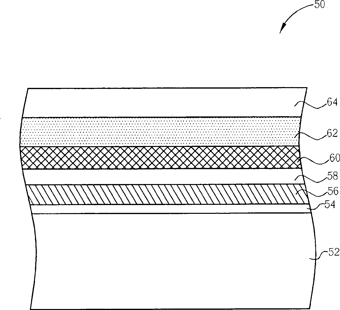
[0031] Please refer to Figure 3 to Figure 8 , Figure 3 to Figure 8 It is a process schematic diagram of the first embodiment of the method for manufacturing a flash memory 50 of the present invention. The flash memory 50 of the present invention is a split-gate flash memory. First, if image 3 As shown, a semiconductor substrate 52 is provided, which may be a silicon substrate. An oxidation process is then performed to form an oxide layer on the surface of the semiconductor substrate 52 as the floating gate dielectric layer 54 . Next, a floating gate material layer 56, a dielectric layer 58, a control gate material layer 60, a metal silicide layer 62, and a hard mask layer 64 are sequentially formed on the surface of the semiconductor substrate 52, wherein the floating The gate material layer 56 and the control gate material layer 60 preferably comprise a polysilicon material layer, the metal silicide layer 62 may comprise a tungsten silicide material, the hard mask laye...


PUM


Abstract

The invention provides a method for manufacturing a flash memory, comprising the steps: a floating grid dielectric layer, a floating grid material layer, a dielectric layer, a control grid material layer, a metal silicide layer and a hard mask layer are sequentially formed on the surface of a semiconductor substrate, and then the hard mask layer is patterned; after that, the metal silicide layer, the control grid material layer, the dielectric layer and the floating grid dielectric layer which are covered by the hard mask layer are removed to form a stacking structure, the a silicon covering layer is formed to cover on the surface of the stacking structure, and then a thermal technique is carried out.

Description

technical field [0001] The invention provides a method for manufacturing a flash memory, especially a method for making a flash memory that utilizes a silicon protective layer to improve the structure and operation quality of the memory. Background technique [0002] Non-volatile memory has the characteristics of repeated erasing and reading and writing, coupled with fast transmission and low power consumption, so it has a wide range of applications and has become an essential component in many information, communication and consumer electronics products. However, in order to provide lightweight and high-quality electronic component products, improving the component integration and quality of non-volatile memory has become the focus of the development of the current information industry and memory manufacturing industry. [0003] According to the number of data bits stored in the unit storage unit, the non-volatile storage unit can be further divided into single-bit storage ...

Claims


Application Information

Patent Timeline
Patent Type & Authority Applications(China)
IPC IPC(8): H01L21/336H01L21/8247
Inventor 罗朝元杨立民王炳尧
Owner POWERCHIP SEMICON CORP
Learn More