Integrated preparation method for integrated circuit and capacitance type micro-silicon microphone single slice as well as chip
A technology of integrated circuits and silicon microphones, which is applied in the field of monolithic integrated chips, can solve problems such as high-temperature processes and achieve high-sensitivity effects
- Summary
- Abstract
- Description
- Claims
- Application Information
AI Technical Summary
Problems solved by technology
Method used
Image
Examples
Embodiment 1
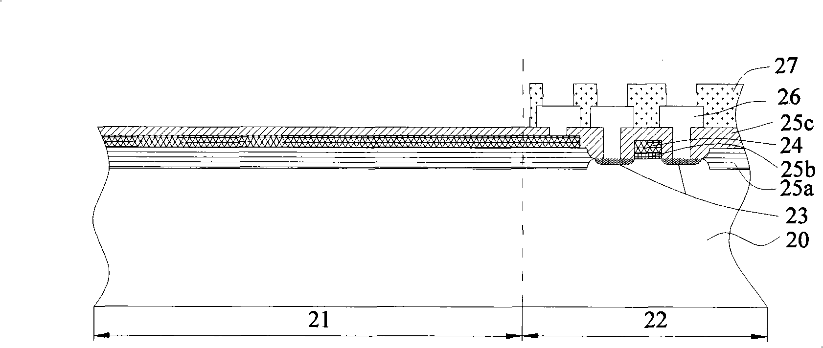
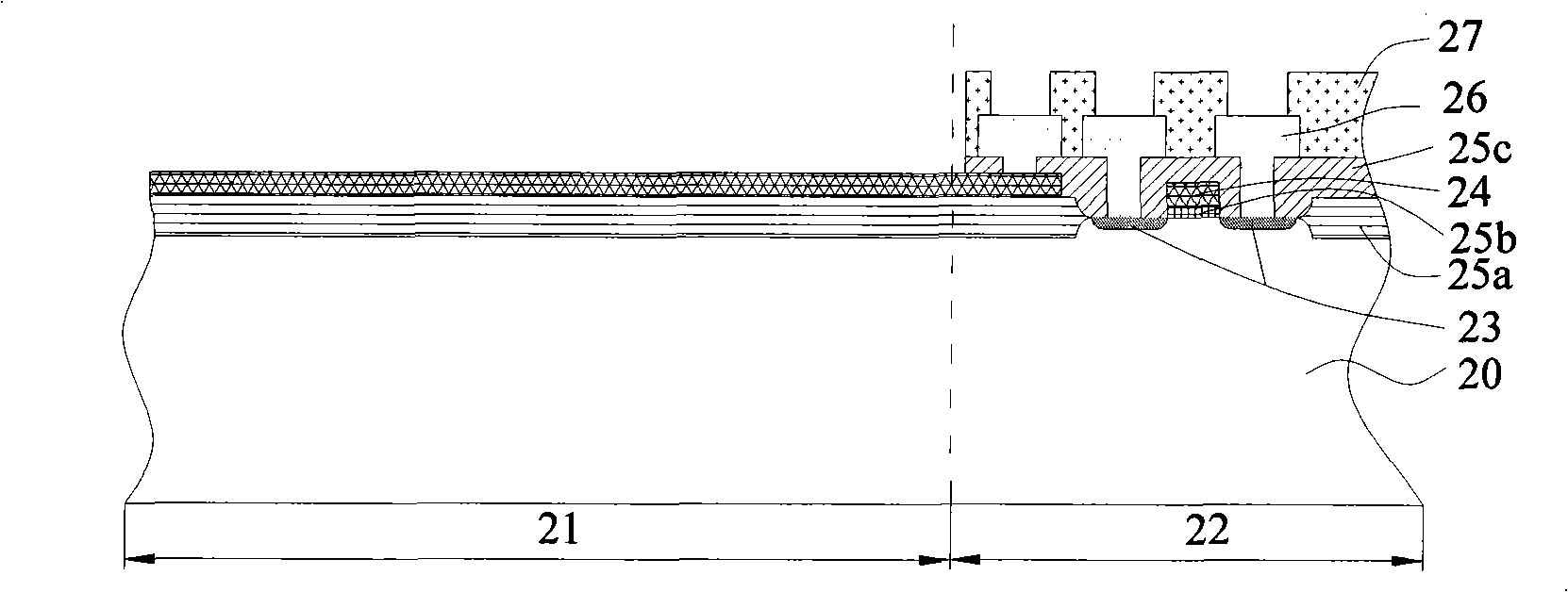
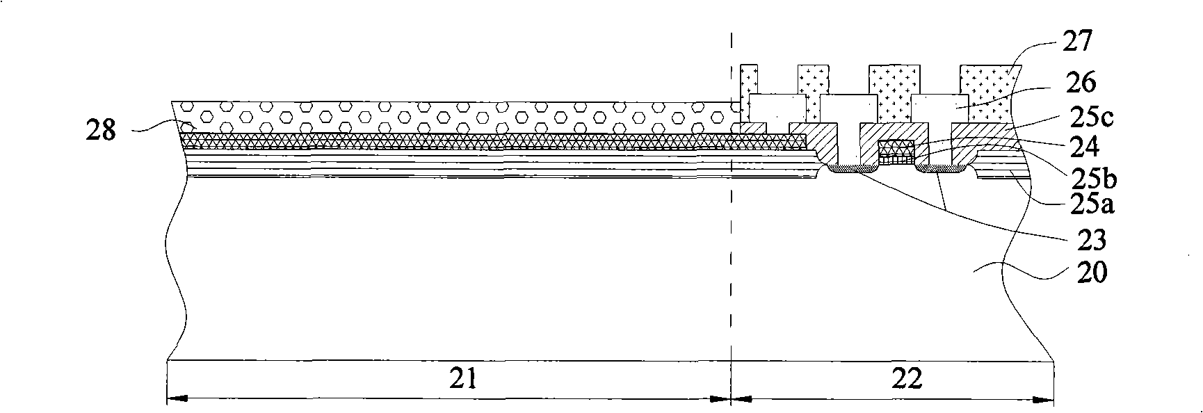
[0038] see Figure 1 to Figure 8 , the manufacturing method of the monolithic integration of the integrated circuit of the present invention and the capacitive micro-silicon microphone mainly comprises the following steps:
[0039] The first step: if figure 1 As shown, a substrate 20 is provided, one surface of which has a first region 22 for forming an integrated circuit and a second region 21 for forming a microsilicon microphone.
[0040] The second step: according to the standard semiconductor process flow, an integrated circuit that is compatible with the micro-silicon microphone is generated in the first region 22, and at the same time, a gate conductive layer 24 is formed in the second region 21 and covers the gate conductive layer 24 The dielectric insulating layer 25c of the integrated circuit can be a field effect transistor, a resistor and a capacitor, etc. For the sake of simplification, the integrated circuit is only described by taking a metal oxide field effec...
Embodiment 2
[0056] See Figure 11 and 12, the manufacturing method of this embodiment is similar to that of Embodiment 1, the difference is that the order of manufacturing the back plate and the sound-sensitive film is adjusted, that is, the first to third steps are executed sequentially according to the foregoing description, and then the fourth step is executed, That is, an additional film (that is, the first film layer 28) is formed on the gate conductive layer located on the second region by using a low-temperature process lower than 400° C. so that the additional film and the gate conductive layer are combined to form a back surface. The pole plate 28c is used as one pole of the capacitor, and then a plurality of air guide holes are formed on the back pole plate 28c by photolithography and corrosion, and then a sacrificial layer is formed on the additional film by a low temperature process, and then a low temperature process is used to form a sacrificial layer on the additional film....
PUM
 Abstract
Description
Claims
Application Information
 - R&D Engineer
- R&D Manager
- IP Professional
- Industry Leading Data Capabilities
- Powerful AI technology
- Patent DNA Extraction
Browse by: Latest US Patents, China's latest patents, Technical Efficacy Thesaurus, Application Domain, Technology Topic, Popular Technical Reports.
© 2024 PatSnap. All rights reserved.Legal|Privacy policy|Modern Slavery Act Transparency Statement|Sitemap|About US| Contact US: help@patsnap.com


