Compensating metal oxide semiconductor image sensor and manufacturing method thereof

An oxide semiconductor and image sensor technology, which is applied in semiconductor/solid-state device manufacturing, semiconductor devices, semiconductor/solid-state device components, etc., can solve problems such as complex processes, improve imaging quality, reduce noise, and improve stability Effect

Inactive Publication Date: 2008-12-24
SEMICON MFG INT (SHANGHAI) CORP
View PDF1 Cites 6 Cited by
  • Summary
  • Abstract
  • Description
  • Claims
  • Application Information

AI Technical Summary

Problems solved by technology

However, this method needs to manufacture a gate layout pattern with a relat

Method used


Image

  • Compensating metal oxide semiconductor image sensor and manufacturing method thereof
  • Compensating metal oxide semiconductor image sensor and manufacturing method thereof
  • Compensating metal oxide semiconductor image sensor and manufacturing method thereof

Examples


Embodiment Construction

[0038] The specific embodiments of the present invention will be described in detail below in conjunction with the accompanying drawings.

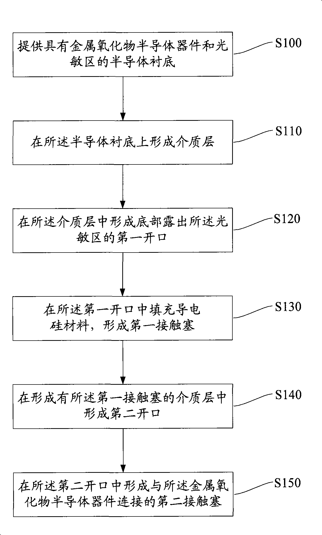
[0039] image 3 It is a flow chart of the first embodiment of the manufacturing method of the CMOS image sensor of the present invention.

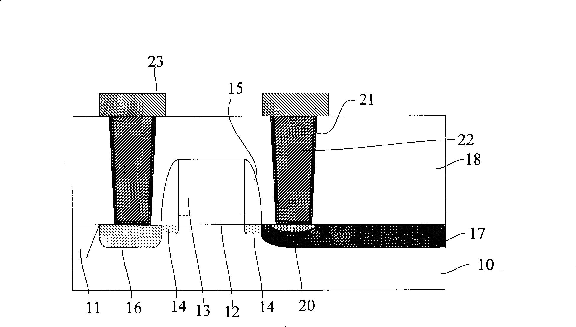
[0040] like image 3 As shown, a semiconductor substrate (S100) with a metal oxide semiconductor device and a photosensitive region is provided, and the semiconductor substrate can be a single crystal silicon material or a polycrystalline silicon material;

[0041] forming a dielectric layer on the semiconductor substrate (S110), the dielectric layer may be silicon oxide or other low dielectric constant material, and the method of forming it may be physical vapor deposition or chemical vapor deposition;

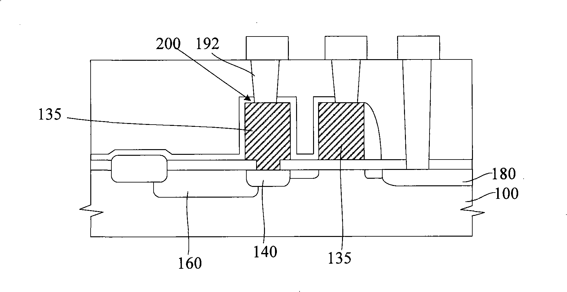
[0042] Form a first opening (S120) whose bottom exposes the photosensitive area in the dielectric layer, the method of forming the first opening may be dry etching, in order to reduce the impact of th...


PUM


Abstract

The invention relates to a method for producing a complementary metal oxide semiconductor image sensor, which comprises the following steps of: providing a semiconductor substrate which is provided with a metallic oxide semiconductor device and a photosensitive area; forming a medium layer on the semiconductor substrate; forming a first opening in the medium layer, wherein, the bottom part of the first opening protrudes from the photosensitive area; forming a first contact stopper by filling a conductive silicon material in the first opening; forming a second opening in the medium layer where the first contact stopper is formed; and forming a second contact stopper connected with the metallic oxide semiconductor device in the second opening. The invention also provides the complementary metal oxide semiconductor image sensor. The invention can reduce the leakage current of the complementary metal oxide semiconductor image sensor and enhance the performance of the device.

Description

technical field [0001] The invention relates to the technical field of semiconductor manufacturing, in particular to a complementary metal oxide semiconductor image sensor and a manufacturing method thereof. Background technique [0002] Complementary Metal-Oxide-Semiconductor Image Sensor (CMOS Image Sensor) is widely used in devices such as digital cameras, video cameras, handheld computers, and camera phones due to its low power consumption and high response rate. In general, its main principle is: receiving an optical signal through a photosensitive unit and converting the optical signal into an electrical signal, and then further processing the electrical signal through a metal oxide semiconductor device. figure 1 It is a schematic cross-sectional structure diagram of an existing CIS. Its manufacturing method is as follows: first form shallow trench isolation region 11 on semiconductor substrate 10, define active area; Form oxide layer 12 on semiconductor substrate 10 ...

Claims


Application Information

Patent Timeline
IPC IPC(8): H01L21/822H01L21/768H01L27/146H01L23/522H01L23/532
Inventor 杨承罗飞徐锦心朱虹
Owner SEMICON MFG INT (SHANGHAI) CORP
Why Eureka
Try Eureka