
Process for effectively controlling air bubble producing in forming process of fluorine-containing silex glass interlayer medium layer

A technology of interlayer dielectric layer and silicate glass layer, applied in the direction of glass/slag layered products, layered products, metal layered products, etc., can solve the problem of interlayer dielectric layer performance damage, damage, and inability to fully function Prevent problems such as metal layer short circuit

Inactive Publication Date: 2008-10-22
SEMICON MFG INT (SHANGHAI) CORP
View PDF0 Cites 4 Cited by
  • Summary
  • Abstract
  • Description
  • Claims
  • Application Information

AI Technical Summary

Problems solved by technology

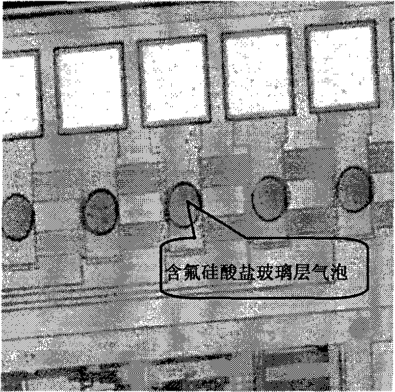
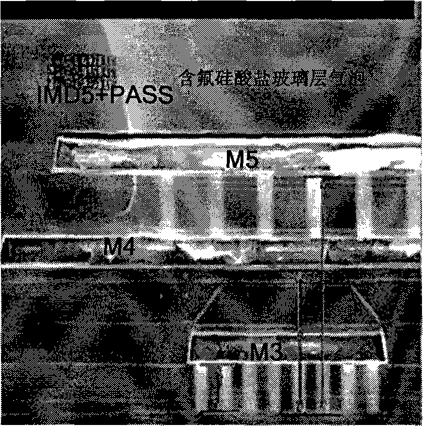
Bubbles in the interlayer dielectric layer of fluorine-containing silicate glass cause damage to the performance of the interlayer dielectric layer, and the interlayer dielectric layer cannot completely prevent the short circuit of the adjacent metal layer, resulting in a decrease in the performance of the semiconductor device or even damage

Method used


Image

  • Process for effectively controlling air bubble producing in forming process of fluorine-containing silex glass interlayer medium layer
  • Process for effectively controlling air bubble producing in forming process of fluorine-containing silex glass interlayer medium layer
  • Process for effectively controlling air bubble producing in forming process of fluorine-containing silex glass interlayer medium layer

Examples


Embodiment Construction

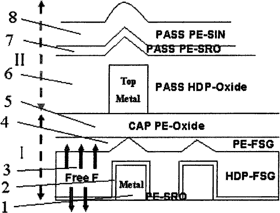
[0026] According to the method of effectively controlling the bubbles generated in the formation of the fluorine-containing silicon glass interlayer dielectric layer of the present invention, the final interlayer dielectric layer (I) with a three-layer structure and the last protective layer (II) with a three-layer structure are formed , A capacitor PE-Oxide dielectric layer is formed between the last interlayer dielectric layer (I) and the last protective layer (II), so it can prevent fluorine ions from escaping from the fluorine-containing silicon glass interlayer dielectric layer and prevent semiconductor device performance damage, which improves the product qualification rate of semiconductor devices. Such as image 3 Displayed, in order from bottom to top, includes:

[0027] Step 1, before forming the final fluorine-containing silicate glass interlayer dielectric layer on the metal layer (1), first form PE-SRO (plasma-enhanced silicon-rich silicon glass) with high dielec...


PUM

PropertyMeasurementUnit
thicknessaaaaaaaaaa

Abstract

According to a method of the invention that air bubble is effectively controlled to be produced in the formation of an inter-layer medium layer of fluorine-contained silicon glass, a final inter-layer medium layer (I) with three-layer structure is formed and an HDP-SRO layer (9) is formed on a formed PE-Oxide medium layer of a capacitor before a final protection layer (II) with three-layer structure is formed, which causes the existing final protection layer (II) formed with three-layer structure to become a final protection layer (III) with fourth-layer structure by adding the HDP-SRO layer (9), thus preventing fluorine ions from escaping from the inter-layer medium layer of the fluorine-contained silicon glass and improving the product percent of pass.

Description

technical field [0001] The invention generally relates to a manufacturing method of a semiconductor device, in particular to a method for effectively controlling bubbles generated during the formation of a fluorine-containing silicon glass interlayer dielectric layer. Background technique [0002] As is well known to those skilled in the art, a semiconductor device has a multi-layer film structure, including multiple metal layers and multiple dielectric layers and protective layers. The metal layer therein constitutes the metal connection lines in the semiconductor device. In order to prevent short circuits between adjacent metal layers, an interlayer dielectric layer is placed between adjacent metal layers. The interlayer dielectric layer is usually formed by depositing a layer of fluorine-containing silicate glass by high-density plasma. [0003] However, if the interlayer dielectric layer containing fluorine-silicate glass is formed by high-density plasma deposition, af...

Claims


Application Information

Patent Timeline
Patent Type & Authority Applications(China)
IPC IPC(8): C03C17/34B32B7/02B32B15/04B32B17/06H01L21/76
Inventor 陈建维刘崇志李景伦周俊
Owner SEMICON MFG INT (SHANGHAI) CORP
Learn More