Semiconductor radiation detector with high resolution

A nuclear radiation detector and high-resolution technology, applied in the field of improved silicon drift semiconductor detectors, can solve the problems of reducing the output capacitance of the detector, distorting the electric field, affecting the shape of the X-ray energy spectrum, etc., and achieving the effect of avoiding adverse effects

Active Publication Date: 2008-10-08
JIANGSU SKYRAY INSTR
View PDF0 Cites 9 Cited by
  • Summary
  • Abstract
  • Description
  • Claims
  • Application Information

AI Technical Summary

Problems solved by technology

[0018] 1) Since the first-stage FET is integrated in the detector and is located in the center of the detector, the electric field below the FET will be distorted, resulting in the loss of signal electrons generated by incident X-rays and affecting the shape of the X-ray energy spectrum (especially low energy background)
Although the area occupied by this effect tube is very small, it will affect the resolution and peak-to-background ratio of the detector after all.
[0019] 2) Since the P-type drift electrode is a concentric ring structure, the signal electrons generated by the X-rays incident on the detection area of ​​the detector drift along all directions to the anode located in the central ring, and the output capacitance of the detector there is a possibility of reduction

Method used


Image

  • Semiconductor radiation detector with high resolution
  • Semiconductor radiation detector with high resolution
  • Semiconductor radiation detector with high resolution

Examples


Embodiment Construction

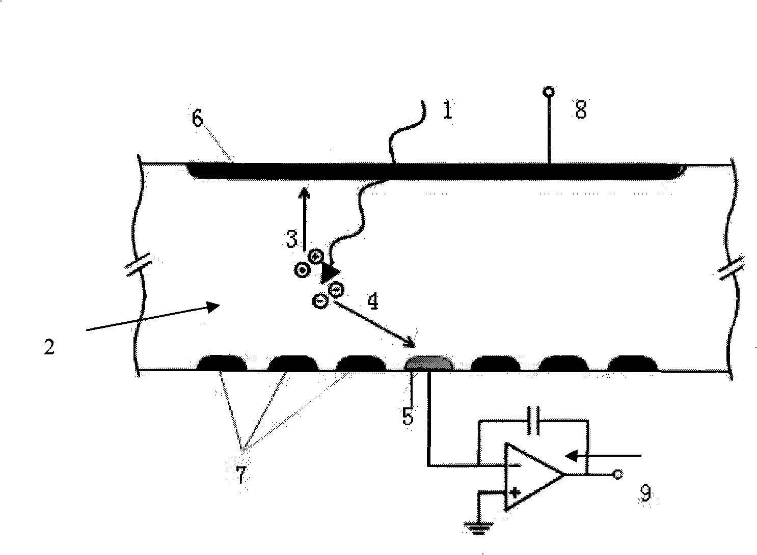
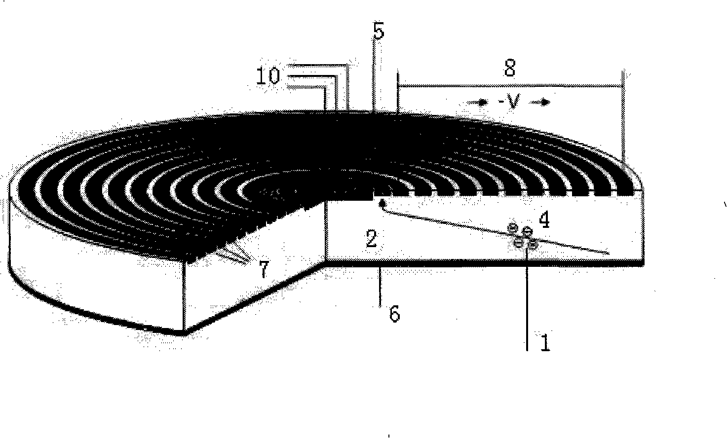
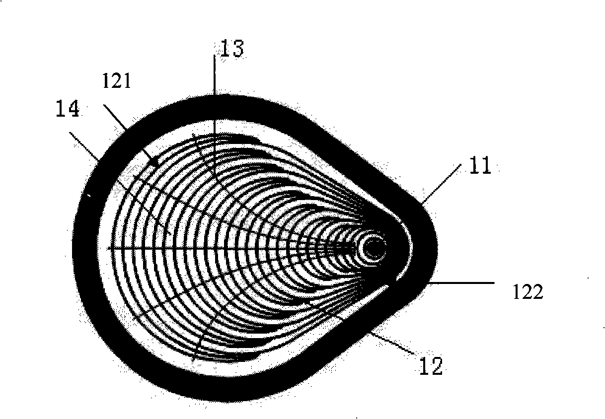
[0037] Further illustrate the present invention below in conjunction with accompanying drawing and embodiment, as image 3 with Figure 4 As shown, a high-resolution semiconductor nuclear radiation detector (UHRD) includes a high-resistance N-type semiconductor silicon wafer, a detection intrinsic region, a point-like N-type anode (16) and a first-stage field effect transistor (11 ), a convex ring-shaped P-type drift electrode (12), the semiconductor silicon wafer is circular, and the backside area (14) of the incident X-ray detection intrinsic region is where the large circle of the convex ring P-type drift electrode is located Therefore, the detection intrinsic region is the region between (14) and the P-N junction of the ray incident surface; the point-shaped N-type anode (11) is located at the back of the incident X-ray detection intrinsic region The area outside the area (14) is surrounded by the P-type drift electrodes (12) with the N-type anode as the focus, and the P-...


PUM


Abstract

A semiconductor radiation detectors with high-resolution, which includes a semiconductor silicon with high purity and N type, a detection intrinsic region, a N type point anodic, a P type drift electrode and a first field-effect transistor, the semiconductor silicon (namely base chip) is of square shaped, the detection intrinsic region is consist of a P-N knot which evenly placed in the ray incident surface of the semiconductor silicon with high purity and N type, the N type point anodic is located outside of the intrinsic region relative to a side, and is surrounded by the P type drift electrode whose focus is a N type electrode, the P type drift electrodes are a plurality of article round convex rings whose focus is the N type electrode, the first filed-effect transistor is arranged inside the N type electrode. A new planar construction of the P type drift electrode is used in the detector on the base of silicon drift detector SDD, and key progress is processed for maintaining high resolution in SDD, large counting region, small size, light weight, and weak points of the SDD existed in the past is quite improved.

Description

technical field [0001] The invention relates to a semiconductor nuclear radiation detector used in an X-ray fluorescence spectrometer (hereinafter referred to as XRF), especially an improved silicon drift semiconductor detector with ultra-high resolution (hereinafter referred to as UHRD). Background technique [0002] The present invention is mainly aimed at the key core component in the energy dispersive X-ray fluorescence spectrometer (hereinafter referred to as EDXRF)-semiconductor nuclear radiation detector. [0003] EDXRF uses X-rays to irradiate the sample, the elements contained in it are excited, and the fluorescent X-rays produced have the characteristics of different energies, which are separated and detected by the energy resolution and proportional working characteristics of the detector, so as to calculate the X-rays in the sample. Instruments for the content of elemental components. The detector is a key component in the EDXRF system, and its performance is cr...

Claims


Application Information

Patent Timeline
Patent Type & Authority Applications(China)
IPC IPC(8): G01N23/223G01T1/24
CPCH01L31/115H01L31/035281H01L31/18Y02E10/50
Inventor 姚栋樑李胜辉
Owner JIANGSU SKYRAY INSTR
Why Eureka
Try Eureka