Transparent conductive polymer as amorphous silicon battery p layer

A technology for hydrogenating amorphous silicon and transparent metals, applied in the field of solar energy materials, can solve the problems of reducing photocurrent collection efficiency, increasing p-layer resistance, and increasing resistivity

Inactive Publication Date: 2008-08-20
BEIJING XINGZHE MULTIMEDIA TECH
View PDF0 Cites 2 Cited by
  • Summary
  • Abstract
  • Description
  • Claims
  • Application Information

AI Technical Summary

Problems solved by technology

[0008] Unfortunately, for the wide-bandgap amorphous silicon alloy p-layer, the wider bandgap and lower optical losses lead to resistance due to the contact barrier between the interface and the transparent conductive oxide front electrode (front contact layer). The rate of increase and the internal resistance of the p-layer increase, thereby reducing the collection efficiency of photocurrent
These are the fundamental limitations of the performance of traditional silicon thin-film solar cells

Method used


Image

  • Transparent conductive polymer as amorphous silicon battery p layer

Examples


Embodiment Construction

[0017] A representative method for forming conductive polymers is to use vacuum coating to produce p-type conductive polymers with a thickness in the range of 10-30 nanometers at a temperature not exceeding 300 ° C, including nitrogen-sulfur long Polymers composed of chain polymers and hydrocarbons.

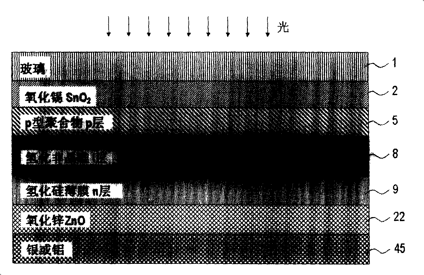
[0018] The above-mentioned p-type conductive polymer can be used as the p-layer of p-i-n-type amorphous silicon solar cells to reduce light absorption loss, thereby increasing its output power. As shown in the accompanying drawings, the structure of this type of cell includes a first layer or substrate 1 with high transparency and structural stability, a transparent conductive oxide front electrode 2 (front contact layer) formed on the substrate, a A p-layer 5 made of conductive polymer, an i-layer 8 made of non-doped hydrogenated amorphous silicon, a phosphorus-doped n-layer 9 based on hydrogenated silicon thin film, another transparent conductive film 22, a metal film 45. In ...


PUM

PropertyMeasurementUnit
Thicknessaaaaaaaaaa
Thicknessaaaaaaaaaa
Thicknessaaaaaaaaaa

Abstract

The present invention discloses application of p type polymer film in amorphous silicon photovoltaic device. The 10-30 nanometer transparent p type polymer produced by vacuum coating can be used as p layer of p-i-n type amorphous silicon solar cell to reduce light absorption loss and improve output power.

Description

technical field [0001] The invention belongs to the field of solar energy materials, and in particular relates to material technology applied to thin-film photovoltaic devices. Background technique [0002] In recent years, the development of thin-film solar photovoltaic cells and large-area modules or templates (photovoltaic modules) has attracted worldwide attention. The great potential of hydrogenated amorphous silicon, especially nanocrystalline silicon (nano-silicon) for wide application in commercial and residential optoelectronic devices has been shown. An important feature of hydrogenated silicon thin-film optoelectronic devices made at a temperature below 260°C is the use of cheap thin-film substrate materials and superb processing methods and equipment when depositing the semiconductor silicon thin film and electrical contact layer over a large area , so that it has the advantages of low production cost and excellent performance at the same time. The laser scribi...

Claims


Application Information

Patent Timeline
IPC IPC(8): H01L51/42H01L51/46
CPCY02E10/549
Inventor 李沅民马昕
Owner BEIJING XINGZHE MULTIMEDIA TECH
Why Eureka
Try Eureka