Lead-free metallic material for electronic component
A lead-free solder and product technology, used in welding/welding/cutting items, welding media, welding equipment, etc. Problems such as wire drawing, deterioration of mechanical properties and plastic workability, etc., to achieve the effect of improved welding bond strength and reliability, excellent oxidation resistance, good bond strength and reliability
- Summary
- Abstract
- Description
- Claims
- Application Information
AI Technical Summary
Problems solved by technology
Method used
Image
Examples
Embodiment 1
[0073] A lead-free solder consisting of tin-9.0 wt% zinc-0.1 wt% tantalum was melted and the melt was cast into a billet with a diameter of 100 mm and a length of 300 mm. The billets were then extruded into rods 10 mm thick and 70 mm wide. The bars were then rolled to form strips 100 μm thick and 70 mm wide.
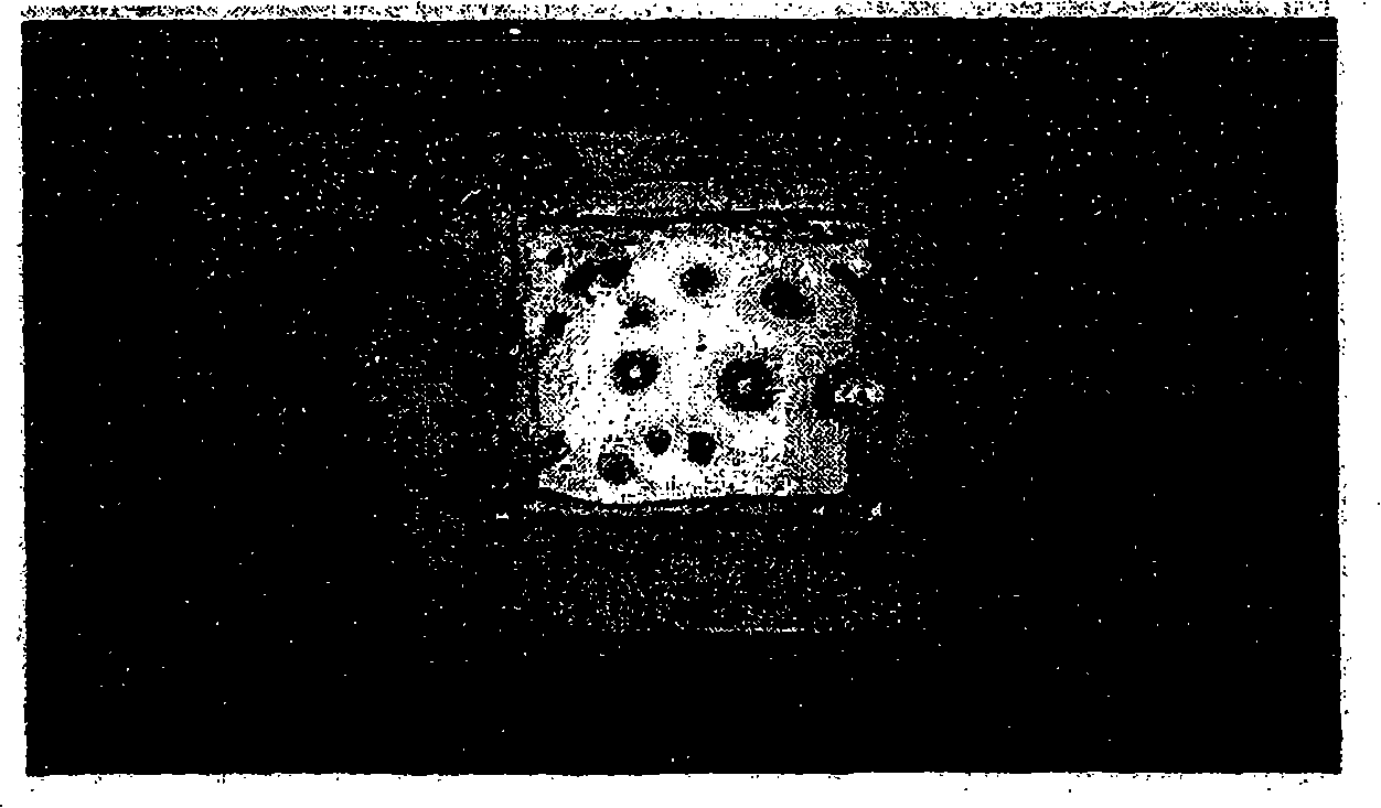
[0074] Then, as shown in FIG. 7, flux is coated on the surface of the copper plate 100 with a thickness of 3 mm, a width of 50 mm, and a length of 60 mm shown in FIG. Coated copper plate 100. Next, a copper-plated SiN substrate 101 having a thickness of 0.5 mm, a width of 30 mm, and a length of 40 mm was placed on the upper portion of the ribbon-shaped solder 102 . The assembly was heated for 45 seconds at a temperature of 230° C. in a nitrogen atmosphere to reflow. Thermal cycle tests were performed on the connection products thus obtained at temperatures ranging from -25°C to 125°C. After 2,000 cycles of thermal cycle testing, connected products are tested with ult...
Embodiment 2
[0076] A lead-free solder consisting of tin-0.5wt% copper-2.5wt% silver-4.0wt% indium-0.1wt% tantalum-0.1wt% cobalt was melted and the melt was cast into a billet with a diameter of 100 mm and a length of 300 mm. The billets were then extruded into rods 10 mm thick and 70 mm wide. The bars were then rolled to form strips 100 μm thick and 70 mm wide.
[0077] Then, as shown in Figure 7, flux is coated on the surface of the copper plate 100 of thick 3mm, wide 50mm, long 60mm, then the strip solder 102 of thick 100 μm, wide 40mm, long 50mm is placed on the copper plate that has been coated. 100 on. Next, a copper-plated SiN substrate 102 having a thickness of 0.5 mm, a width of 30 mm, and a length of 40 mm was placed on the upper portion of the ribbon-shaped solder 101 . The assembly was heated at a temperature of 250° C. in a nitrogen atmosphere for 45 seconds to reflow. Thermal cycle tests were performed on the connection products thus obtained at temperatures ranging from -...
PUM
| Property | Measurement | Unit |
|---|---|---|
| surface tension | aaaaa | aaaaa |
| diameter | aaaaa | aaaaa |
Abstract
Description
Claims
Application Information
 - Generate Ideas
- Intellectual Property
- Life Sciences
- Materials
- Tech Scout
- Unparalleled Data Quality
- Higher Quality Content
- 60% Fewer Hallucinations
Browse by: Latest US Patents, China's latest patents, Technical Efficacy Thesaurus, Application Domain, Technology Topic, Popular Technical Reports.
© 2025 PatSnap. All rights reserved.Legal|Privacy policy|Modern Slavery Act Transparency Statement|Sitemap|About US| Contact US: help@patsnap.com


