Low temperature aerosol deposition of a plasma resistive layer

A technology of air flotation deposition and air flotation, which is used in ion implantation plating, devices for coating liquids on surfaces, coatings, etc.

Active Publication Date: 2008-04-30
APPLIED MATERIALS INC
View PDF0 Cites 12 Cited by
  • Summary
  • Abstract
  • Description
  • Claims
  • Application Information

AI Technical Summary

Problems solved by technology

However, high temperature treatment may invalidate the surface properties or deleteriously modify the microstructure of the coating surface, resulting in coatings with poor uniformity and / or surface cracks due to elevated temperature
Additionally, if the coating, or the underlying surface of that coating, has microcracks or if the coating is applied unevenly, the component surface can become damaged over time and eventually expose the underlying component surface to corrosive plasma bombardment

Method used


Image

  • Low temperature aerosol deposition of a plasma resistive layer

Examples


Embodiment Construction

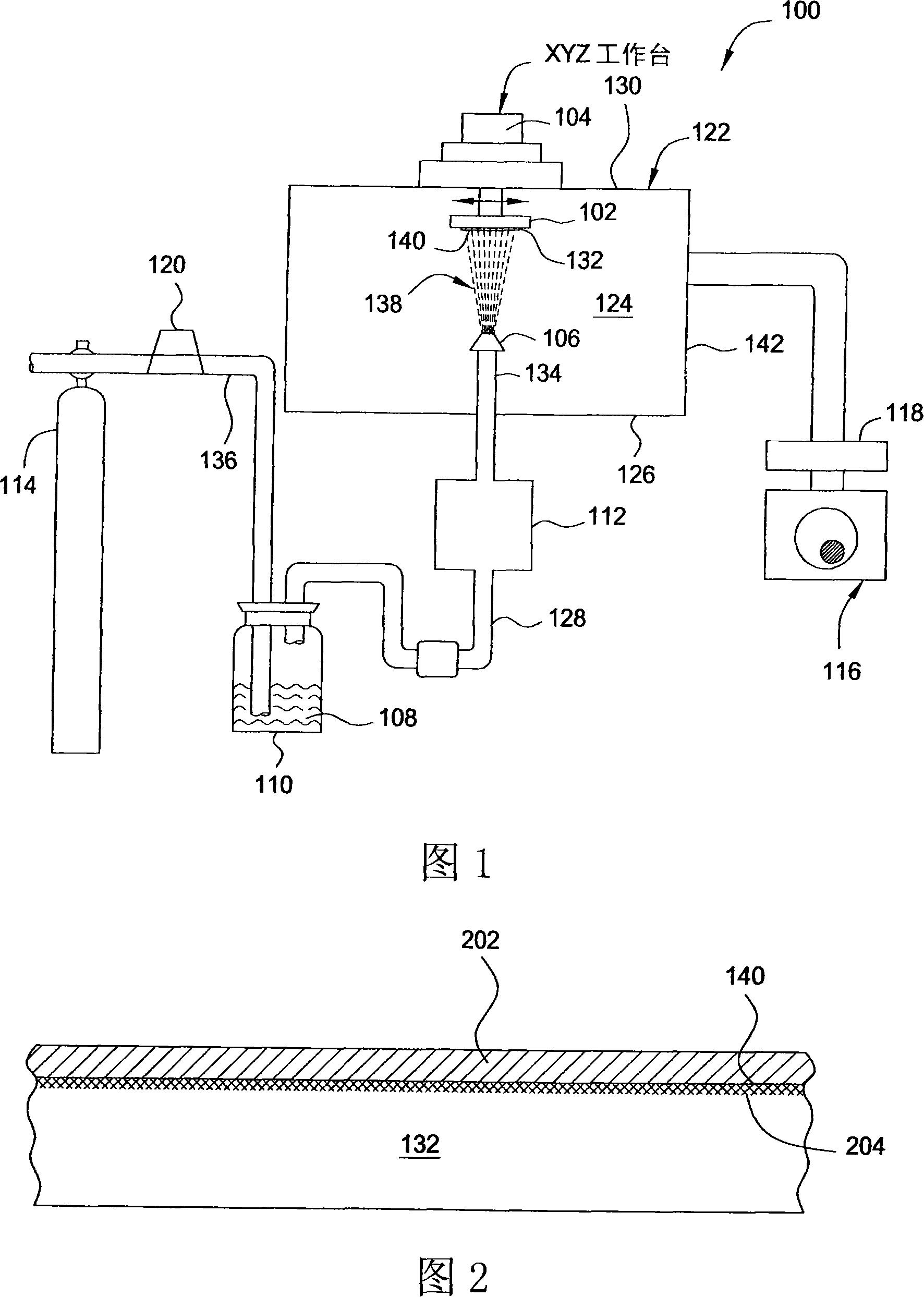
[0014] Figure 1 is a cross-sectional view of one embodiment of an apparatus 100 that may be used to perform an air-lift deposition (AD) process in accordance with the present invention. The air flotation deposition (AD) process of the present invention forms a plasma resistant layer that can be used to advantageously protect surfaces exposed to plasma treatment. Apparatus 100 includes a processing chamber 122 having a top 130 , a bottom 126 and side walls 142 defining a processing zone 124 within the interior of the processing chamber 122 . The workbench 104 is disposed on a ceiling 130 of the processing chamber 122 to a substrate holder 102 that holds a substrate 132 during processing. Table 104 is used to move fixture 102 along the X, Y and Z axes. Accordingly, the stage 104 moves the substrate 132 positioned thereon along the X, Y, and Z axes. Mechanical booster pump 116 and rotary pump 118 are coupled to processing region 124 through ports formed in sidewall 142 of proce...


PUM

PropertyMeasurementUnit
diameteraaaaaaaaaa
diameteraaaaaaaaaa
grain sizeaaaaaaaaaa

Abstract

Embodiments of the present invention provide a method of low temperature air flotation deposition of a plasma resistant layer on semiconductor chamber components / parts. In one embodiment, a method for low temperature air flotation deposition comprises forming an air flotation of fine particles in an air flotation generator, distributing said air flotation from the generator into a processing chamber towards a substrate surface, maintaining the The substrate temperature is between about 0 degrees Celsius and 50 degrees Celsius, and a layer of material from the air flotation is deposited on the substrate surface.

Description

technical field [0001] Embodiments of the present invention relate generally to semiconductor processing and, more particularly, to low temperature air flotation deposition of plasma resistant layers on semiconductor processing chamber components. Background technique [0002] Semiconductor processing involves several different chemical and physical steps that form tiny integrated circuits on a substrate. The layers of various materials making up the integrated circuit are produced by chemical vapor deposition, physical vapor deposition, epitaxial growth, and the like. Partial layers of multiple materials are patterned using photoresist masks and wet or dry etching techniques. The substrates used to form integrated circuits can be silicon, gallium arsenide, indium phosphide, or other suitable materials. [0003] A typical semiconductor processing chamber includes a chamber defining a processing zone, a gas distribution assembly adapted to supply gas from a gas supply to th...

Claims


Application Information

Patent Timeline
Patent Type & Authority Applications(China)
IPC IPC(8): C23C24/08B05D1/12H01L21/02
CPCC23C14/564C23C24/04C23C16/4404H01L21/20H01L21/02
Inventor 珍妮弗·Y·孙埃尔米拉·赖亚博瓦塞恩·撒奇熹·朱西姆仁·L·卡茨
Owner APPLIED MATERIALS INC
Why Eureka
Try Eureka