
Tunnel transistor having spin-dependent transfer characteristic and nonvolatile memory using same

A transistor and tunnel barrier technology, applied in the field of new transistors, can solve problems such as high-density integration difficulties

Inactive Publication Date: 2008-04-09
JAPAN SCI & TECH CORP
View PDF0 Cites 2 Cited by
  • Summary
  • Abstract
  • Description
  • Claims
  • Application Information

AI Technical Summary

Problems solved by technology

If it is desired to achieve a high integration level of more than several gigabits, the channel length of the MOS transistor is expected to be less than 0.1 μm. Routing takes up cell area, making it difficult to integrate the two at high density

Method used


Image

  • Tunnel transistor having spin-dependent transfer characteristic and nonvolatile memory using same
  • Tunnel transistor having spin-dependent transfer characteristic and nonvolatile memory using same
  • Tunnel transistor having spin-dependent transfer characteristic and nonvolatile memory using same

Examples


Embodiment Construction

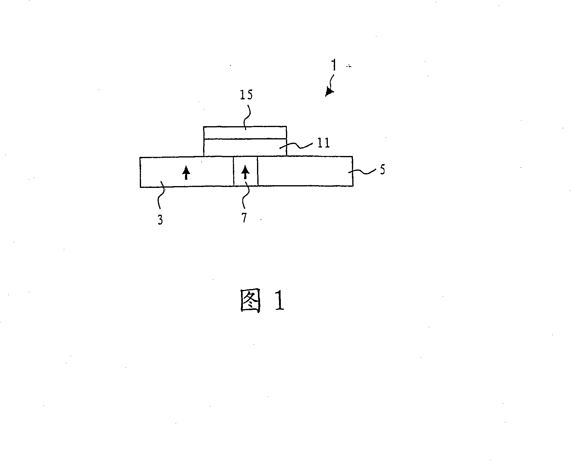
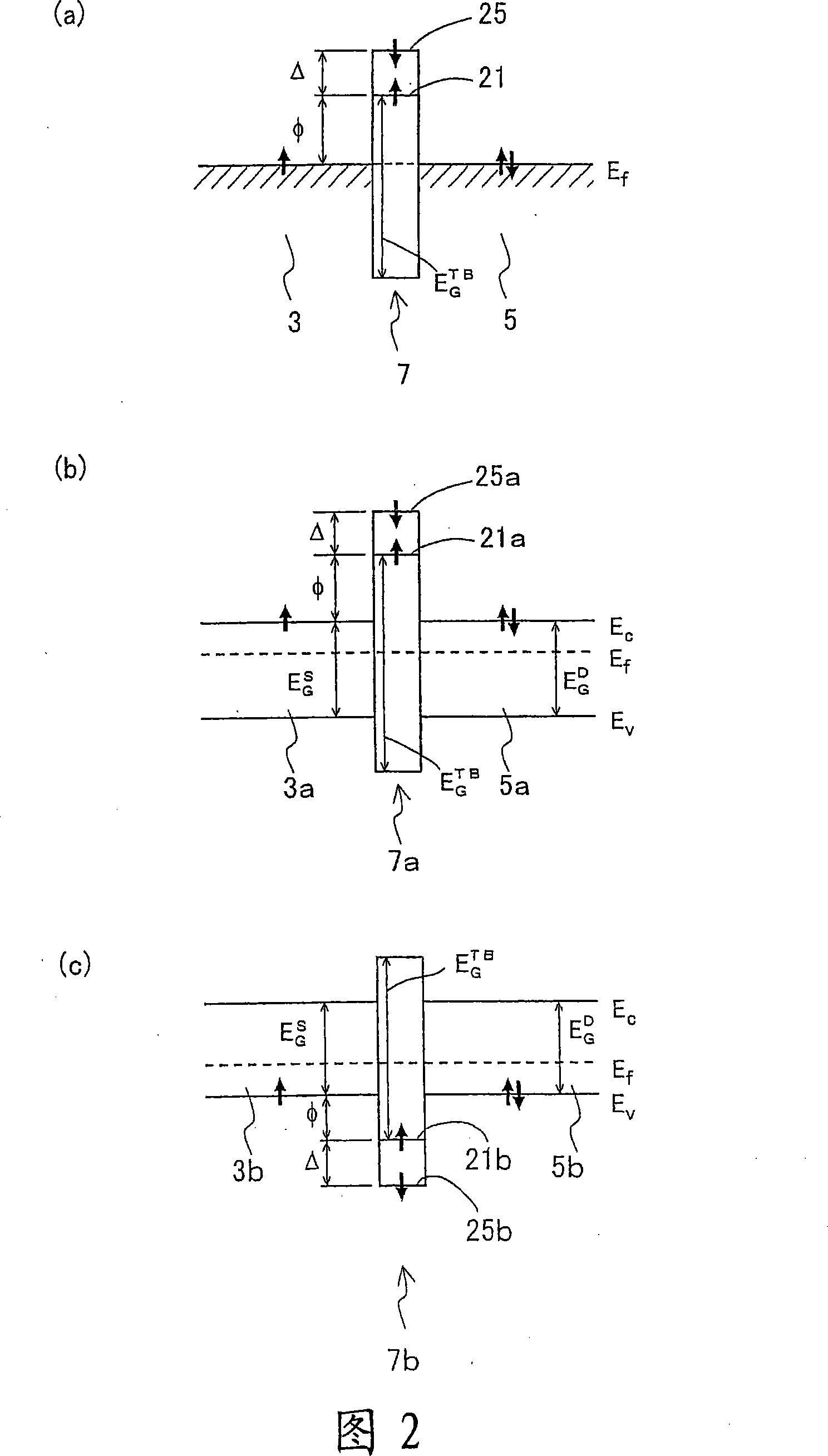
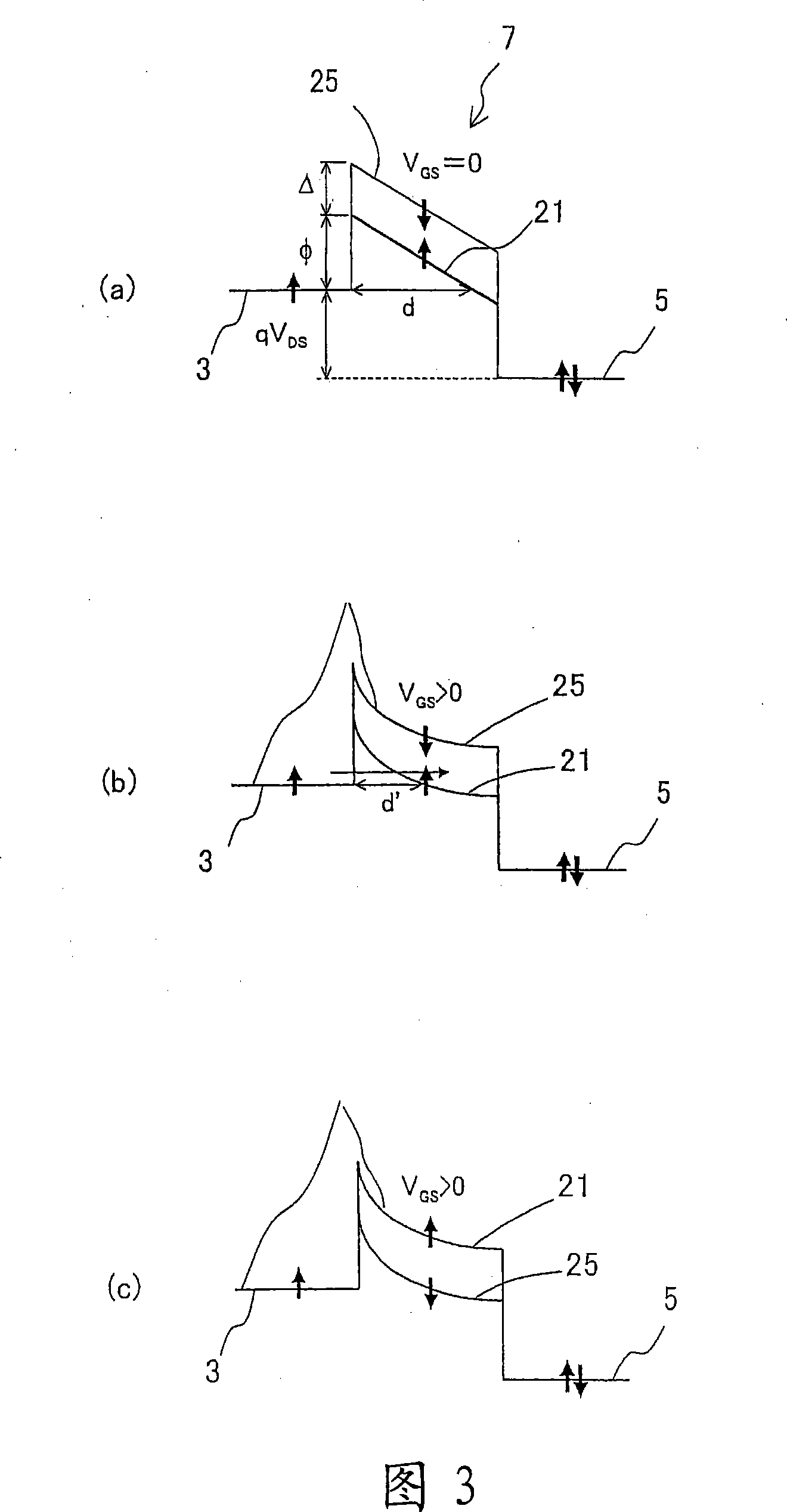
[0071] The transistor according to the first aspect of the present invention is a novel transistor utilizing the spin-dependent tunneling effect of the junction of a ferromagnetic source and a ferromagnetic tunnel barrier. More specifically, it is a tunnel junction including a ferromagnetic tunnel barrier sandwiching insulation between ferromagnetic sources and drains, and a gate electrode that forms the ferromagnetic tunnel barrier and can apply an electric field to the ferromagnetic tunnel barrier formed transistors.

[0072] Also, the term "spin" is usually used for spin angular momentum, but below it is also often used in the sense of a carrier having a specific spin orientation. In addition, it is assumed that the magnetization direction of the ferromagnetic tunnel barrier is determined by the spin direction of the spin band at the band end (for example, the band end of the conduction band and the spin band at the band end of the ferromagnetic tunnel barrier during spin s...


PUM


Abstract

A MISFET the channel region of which is a ferromagnetic semiconductor has a feature that the drain current can be controlled by the gate voltage and a feature that the transfer conductance can be controlled by the relative directions of magnetization in the ferromagnetic channel region and the ferromagnetic source (or the ferromagnetic drain, or both the ferromagnetic source and ferromagnetic drain). As a result, binary information can be stored in the form of the relative magnetization directions, and the relative magnetization directions are electrically detected. If the magnetism is controlled by the electric field effect of the channel region of a ferromagnetic semiconductor, the current needed to rewrite the information can be greatly reduced. Thus, the MISFET can constitute a high-performance nonvolatile memory cell suited to high-density integration.

Description

[0001] This application is an invention patent application with the original application number 200480008988.0 (international application number: PCT / JP2004 / 004512, application date: March 30, 2004, invention name: Tunnel transistor with spin-dependent transfer characteristics and its use Divisional application for non-volatile memory). technical field [0002] The present invention relates to a novel transistor, and more specifically, to a transistor having spin-dependent transfer characteristics and a nonvolatile memory circuit (nonvolatile memory) using the same. Background technique [0003] In recent years, the development of a highly informationized society has attracted attention, and especially recently, "portable devices" as a medium are rapidly expanding. Although it is being recognized that the large demand for "portable equipment" will become the need of the semiconductor industry in the future, corresponding to this, in addition to the high-speed, low-power cons...

Claims


Application Information

Patent Timeline
Patent Type & Authority Applications(China)
IPC IPC(8): H01L29/66H01L27/22H01L23/522H01L21/8246H10N50/10
CPCH01L29/66984B82Y10/00H01F10/3254H01F10/193B82Y25/00H01L27/228G11C11/16H01F1/405H10B61/22
Inventor 菅原聪田中雅明
Owner JAPAN SCI & TECH CORP
Learn More