Method for preparation of a-b orientated ZnO nanometer linear array
A nanowire array and orientation technology, applied in the fields of nanostructure manufacturing, nanotechnology, nanotechnology, etc., to achieve the effects of easy control of chemical composition, less crystal defects, and excellent UV light sensitivity.
Inactive Publication Date: 2007-09-19
UNIV OF ELECTRONICS SCI & TECH OF CHINA
View PDF0 Cites 13 Cited by
- Summary
- Abstract
- Description
- Claims
- Application Information
AI Technical Summary
Problems solved by technology
Most of the reported preparation methods are c-axis preferred orientation ZnO nano-arrays; and ZnO nano-wire arrays with obvious a-b orientation, that is, ZnO nano-wire arrays with C-axis parallel to the growth of the substrate, have not yet been reported.
Method used
View moreImage
Smart ImageViewing Examples
Examples
Embodiment Construction
Login to View More PUM
| Property | Measurement | Unit |
|---|---|---|
| current | aaaaa | aaaaa |
Abstract
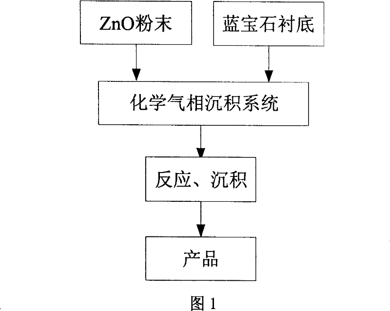
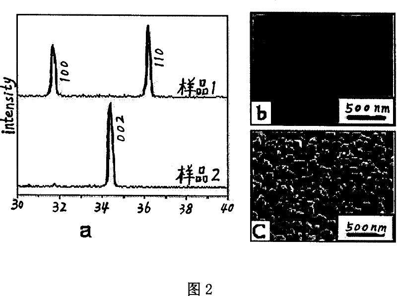
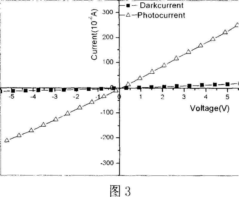
The invention provides a method for preparing ZnO nano line array in a-b orientation which belongs to electronic material technical field, relates to wide bond gap semiconductor ZnO luminescent material, especially relates to a method for preparing ZnO nano line array. The invention uses chemical vapor deposition technique, and employs pure ZnO powder as evaporation source and sapphire Al2O3 (1120) as substrate, and controls the temperature of the evaporation source to be no less than the thermal decomposition temperature of the ZnO powder and the temperature of the substrate to be no less than 750 DEG C. and vacuum degree at 200 to 300 torr, and employs Ar gas as transmission gas with gas flow rate of 35 sccm. In this manner, the ZnO powder is heated to decompose into Zn and O, and then by Ar gas transmission, the ZnO nano line array in a-b orientation is deposited on the substrate. The invention employs current chemical vapor deposition technique, and can easily prepare the ZnO nano line array in a-b orientation which has excellent uv sensitive character and quick light response speed.
Description
technical field The invention belongs to the technical field of electronic materials, and relates to a wide bandgap semiconductor ZnO luminescent material, in particular to a preparation method of a ZnO nanowire array. technical background In recent years, due to its large exciton binding energy (60 mev), ZnO can obtain efficient ultraviolet light emission at room temperature, and has become another research hotspot after GaN materials. Among them, the ZnO nanowire array system is expected to be used as a next-generation nano-optoelectronic device. The first thing that attracts attention is the highly oriented ZnO nanowire array as a natural laser resonator, which can generate ultraviolet laser light when excited, and the ZnO nanowire has an extremely low photoexcitation threshold of 40kW / cm 2 (Thin film material is 300kW / cm 2 ~4MW / cm 2 ), chemical activity and one-dimensional nanostructure, making ZnO nanowires one of the ideal materials for making ultraviolet nanolaser...
Claims
Login to View More Application Information
Patent Timeline
 Patent Type & Authority Applications(China)
IPC IPC(8): H01L31/18H01L21/365C23C16/40C23C16/448B82B3/00C01G9/02
CPCY02P70/50
Inventor 戴丽萍邓宏
Owner UNIV OF ELECTRONICS SCI & TECH OF CHINA
Features
- R&D
- Intellectual Property
- Life Sciences
- Materials
- Tech Scout
- Unparalleled Data Quality
- Higher Quality Content
- 60% Fewer Hallucinations
Learn More Browse by: Latest US Patents, China's latest patents, Technical Efficacy Thesaurus, Application Domain, Technology Topic, Popular Technical Reports.
© 2025 PatSnap. All rights reserved.Legal|Privacy policy|Modern Slavery Act Transparency Statement|Sitemap|About US| Contact US: help@patsnap.com


