Structure and method for controlling the behavior of dislocations in strained semiconductor layers
A semiconductor and control bit technology, applied in semiconductor devices, semiconductor/solid-state device manufacturing, electrical components, etc., can solve the problems of inability to obtain and control the formation of S/D
- Summary
- Abstract
- Description
- Claims
- Application Information
AI Technical Summary
Problems solved by technology
Method used
Image
Examples
Embodiment Construction
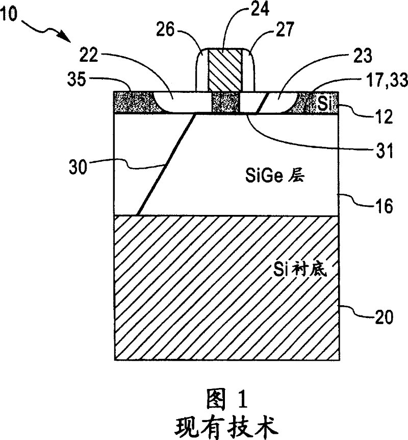
[0017] Figure 1 shows a cross-sectional view of a MOSFET 10 formed on a strained semiconductor layer 12, which is Si or contains Si. Strained layer 12 is formed on SiGe layer 16 , which in turn is formed on substrate 20 . The strained layer 12 may be formed by epitaxial deposition on the SiGe layer 16 . SiGe layer 16 may be formed by epitaxial deposition on substrate 20, which may be single crystal. The amount of germanium in layer 16 increases with the thickness of the layer and then relaxes to form a lattice spacing greater than that of the future lower surface of layer 12 , resulting in a global bidirectional strain in layer 12 . Thus, layer 16 may be graded SiGe, up to upper surface 17 of layer 16 . Layer 12 may be of constant Si or SiGe composition.
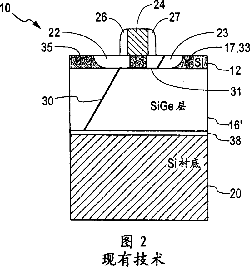
[0018] Alternatively, instead of the SiGe graded layer 16, the layer 16 may be silicon germanium on insulator (SGOI) as shown in FIG. 2 .
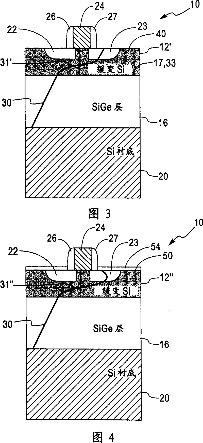
[0019] In FIGS. 1-5 , MOSFET 10 has source 22 , drain 23 and gate 24 . There ar...
PUM
 Abstract
Description
Claims
Application Information
 - R&D
- Intellectual Property
- Life Sciences
- Materials
- Tech Scout
- Unparalleled Data Quality
- Higher Quality Content
- 60% Fewer Hallucinations
Browse by: Latest US Patents, China's latest patents, Technical Efficacy Thesaurus, Application Domain, Technology Topic, Popular Technical Reports.
© 2025 PatSnap. All rights reserved.Legal|Privacy policy|Modern Slavery Act Transparency Statement|Sitemap|About US| Contact US: help@patsnap.com


