Multi-layer heat-insulating membrana paster
A technology of thermal insulation film and patch, applied in layered products, synthetic resin layered products, optics, etc., can solve the problems of reduced thermal insulation effect, hindered signal reception of communication equipment, poor resistance to light, etc.
- Summary
- Abstract
- Description
- Claims
- Application Information
AI Technical Summary
Problems solved by technology
Method used
Image
Examples
Embodiment 1
[0016] Refer to figure 1 The multi-layer heat insulation film patch 1 of this embodiment can be pasted on a substrate 10 such as glass, lens, etc., and includes: a base unit 11, an infrared-resistant layer 12, and a scratch-resistant and wear-resistant layer 13. And an anti-ultraviolet layer 14. The base unit 11 is formed by alternately stacking a plurality of spaced first base films 111 and a plurality of second base films 112 between adjacent first base films 111. The first and second The total number of the two base films 111 and 112 is 100 layers. In general, the base unit 11 has a first surface 113 adjacent to the anti-infrared layer 12 and a second surface 114 adjacent to the anti-ultraviolet layer 14, and The thickness of the outermost layer forming the first or second surface 113, 114 of the aforementioned base film 111, 112 is greater than that located in the middle, and the anti-ultraviolet layer 14 can be directly attached to the substrate 10, and the anti-scratch and w...
Embodiment 2
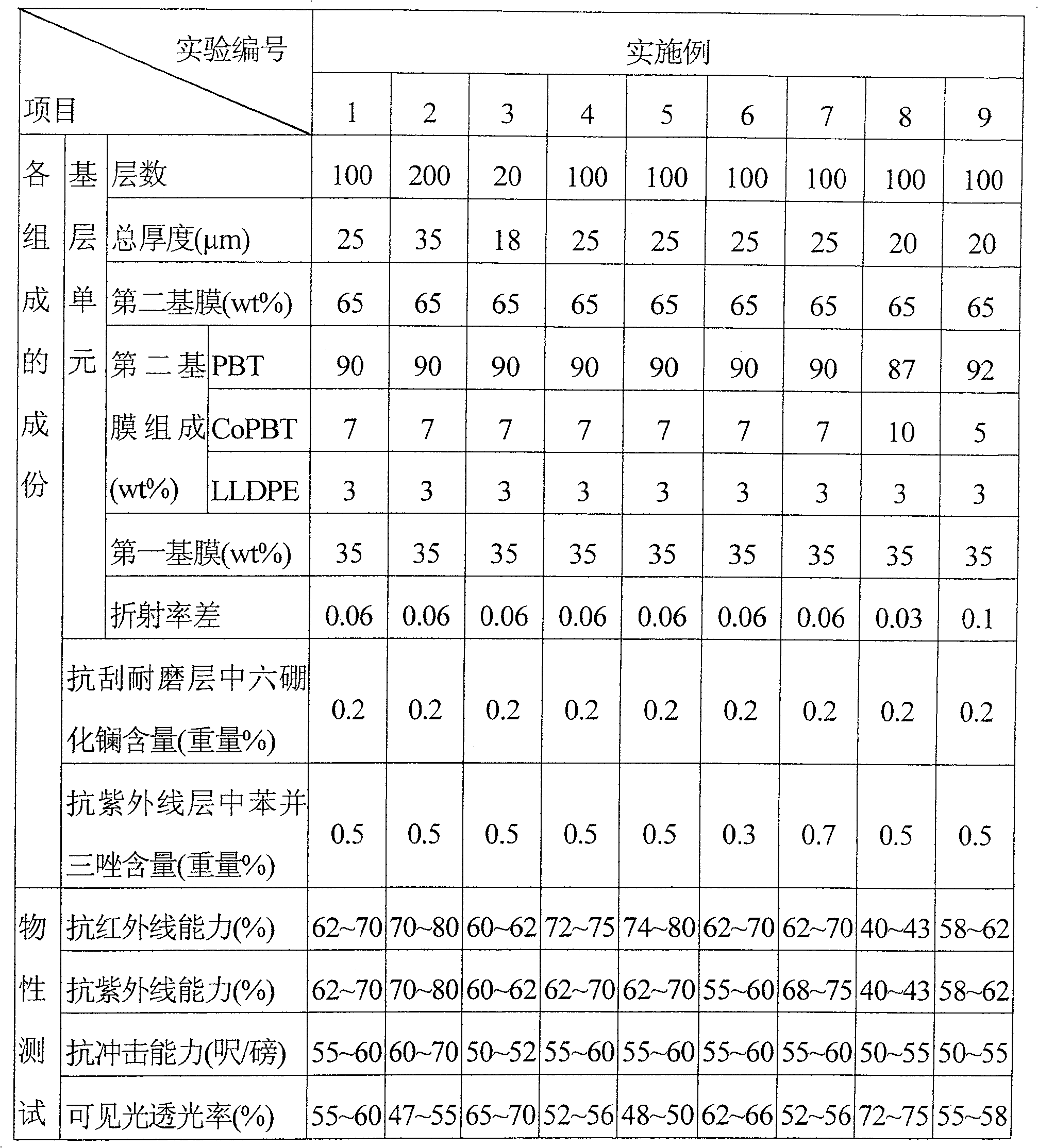
[0024] The composition ratios and processing conditions of the components of Example 2 of the present invention are roughly the same as those of Example 1. The difference is that the number of layers of the base unit 11 is increased to 200. Due to the increase in the number of layers, the total thickness of the base unit 11 Increase to 35μm. After manufacturing, various experiments such as infrared resistance, ultraviolet resistance, impact resistance, and visible light transmittance were also carried out. The experimental results are also shown in Table 1.
Embodiment 3
[0026] The composition ratios and processing conditions of the components of Example 3 of the present invention are also the same as those of Example 1. The difference is that the number of layers of the base unit 11 is reduced to 20, and the overall thickness of the base unit 11 is reduced to 18 μm. After manufacturing, various experiments such as infrared resistance, ultraviolet resistance, impact resistance, and visible light transmittance were also carried out. The experimental results are also shown in Table 1.
PUM
| Property | Measurement | Unit |
|---|---|---|
| particle diameter | aaaaa | aaaaa |
| thickness | aaaaa | aaaaa |
| thickness | aaaaa | aaaaa |
Abstract
Description
Claims
Application Information
 - R&D
- Intellectual Property
- Life Sciences
- Materials
- Tech Scout
- Unparalleled Data Quality
- Higher Quality Content
- 60% Fewer Hallucinations
Browse by: Latest US Patents, China's latest patents, Technical Efficacy Thesaurus, Application Domain, Technology Topic, Popular Technical Reports.
© 2025 PatSnap. All rights reserved.Legal|Privacy policy|Modern Slavery Act Transparency Statement|Sitemap|About US| Contact US: help@patsnap.com


