Exposure apparatus, exposure method, and device fabricating method

An exposure device and exposure beam technology, applied in the field of component manufacturing, can solve problems such as insufficient focus matching and difficulty in matching image planes, and achieve good precision and suppress measurement errors.

Inactive Publication Date: 2009-08-05
NIKON CORP
View PDF33 Cites 0 Cited by
  • Summary
  • Abstract
  • Description
  • Claims
  • Application Information

AI Technical Summary

Problems solved by technology

[0008] If the depth of focus δ becomes too narrow, it will be difficult to align the substrate surface with the image plane of the projection optical system, and the focus matching during exposure operation will be insufficient.

Method used


Image

  • Exposure apparatus, exposure method, and device fabricating method
  • Exposure apparatus, exposure method, and device fabricating method
  • Exposure apparatus, exposure method, and device fabricating method

Examples


Embodiment Construction

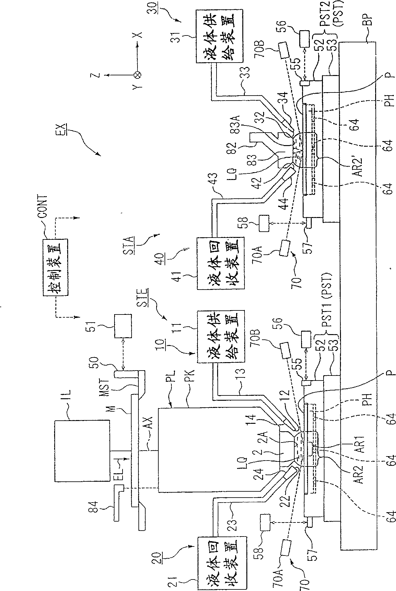
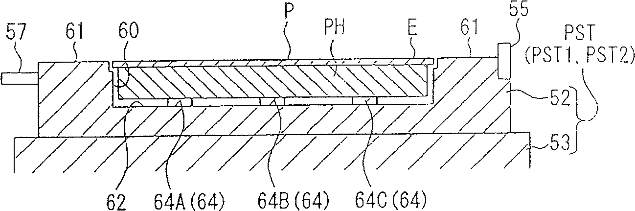
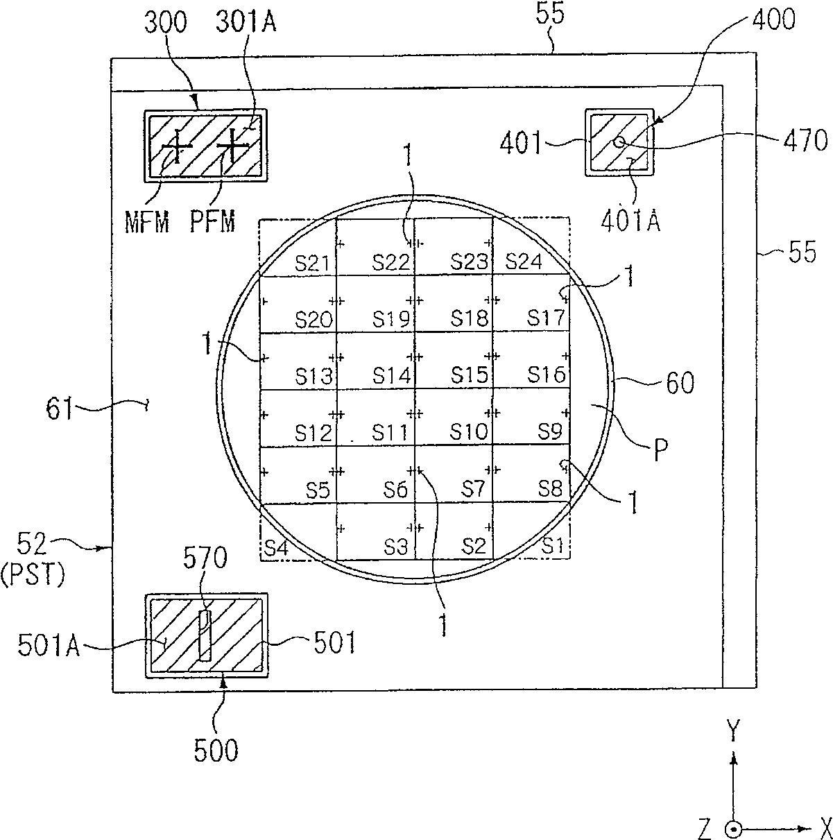
[0053] Hereinafter, the exposure apparatus of the present invention will be described with reference to the drawings. figure 1 It is a schematic configuration diagram showing an embodiment of the exposure apparatus of the present invention.

[0054] figure 1Among them, the exposure apparatus EX is a dual-stage exposure apparatus equipped with two substrate stages, and includes: a first substrate stage PST1 and a second substrate stage PST2 that can move independently on a common base BP, and each can hold And move the substrate P. In addition, this dual-stage exposure apparatus EX includes: an exposure station STE for exposing the substrate P held on the first substrate stage PST1 (or the second substrate stage PST2) through the projection optical system PL and the liquid LQ; The measurement station STA measures the second substrate stage PST2 (or the first substrate stage PST1 ) or the substrate P held on the substrate stage PST2 ( PST1 ).

[0055] By moving the first su...


PUM

PropertyMeasurementUnit
refractive indexaaaaaaaaaa

Abstract

The present invention provides an exposure apparatus capable of performing measurement processing satisfactorily and performing exposure processing with high precision even when a liquid immersion method is applied to a dual stage exposure apparatus. The exposure device (EX) has: at least two substrate stages (PST1, PST2), each of which can hold and move each substrate (P); an exposure station (STE), which uses a projection optical system (PL) and a liquid (LQ ) to expose the substrate (P) held on one of the substrate stages (PST1); The substrate (P) is measured. The measurement at the measurement station (STA) is performed in a state where the liquid (LQ) is arranged on the substrate stage (PST2) or the substrate (P).

Description

technical field [0001] The present invention relates to an exposure device, an exposure method, and an element manufacturing method for exposing a substrate through a liquid. [0002] This application claims priority to Japanese Patent Application No. 2004-42933 filed on February 19, 2004, the content of which is incorporated herein. Background technique [0003] Semiconductor elements or liquid crystal display elements are manufactured by a method called photolithography, which transfers a pattern formed on a photomask to a photosensitive substrate. The exposure device used in the photolithography process has a mask stage for supporting the mask and a substrate stage for supporting the substrate. The mask stage and the substrate stage move sequentially, so that the pattern of the mask is transferred to the substrate by the projection optical system. on the substrate. In recent years, in order to correspond to the pattern integration of higher components, it is expected th...

Claims


Application Information

Patent Timeline
Patent Type & Authority Patents(China)
IPC IPC(8): H01L21/027G03F7/20
CPCG03F9/7096G03F9/7026G03F9/7034G03F7/70341G03F9/7003G03F7/70525G03F7/70783G03F7/70733G03F7/70775
Inventor 堀川浩人
Owner NIKON CORP
Why Eureka
Try Eureka