Semiconductor package substrate increasing static dissipation capability
A technology for packaging substrates and static dissipation. It is used in semiconductor devices, semiconductor/solid-state device components, and electric solid-state devices. It can solve problems such as inconvenience, general products have no structure, and static dissipation has no obvious benefit.
- Summary
- Abstract
- Description
- Claims
- Application Information
AI Technical Summary
Problems solved by technology
Method used
Image
Examples
no. 1 Embodiment
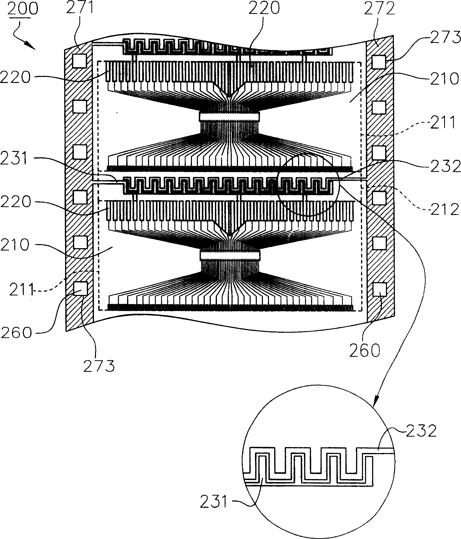
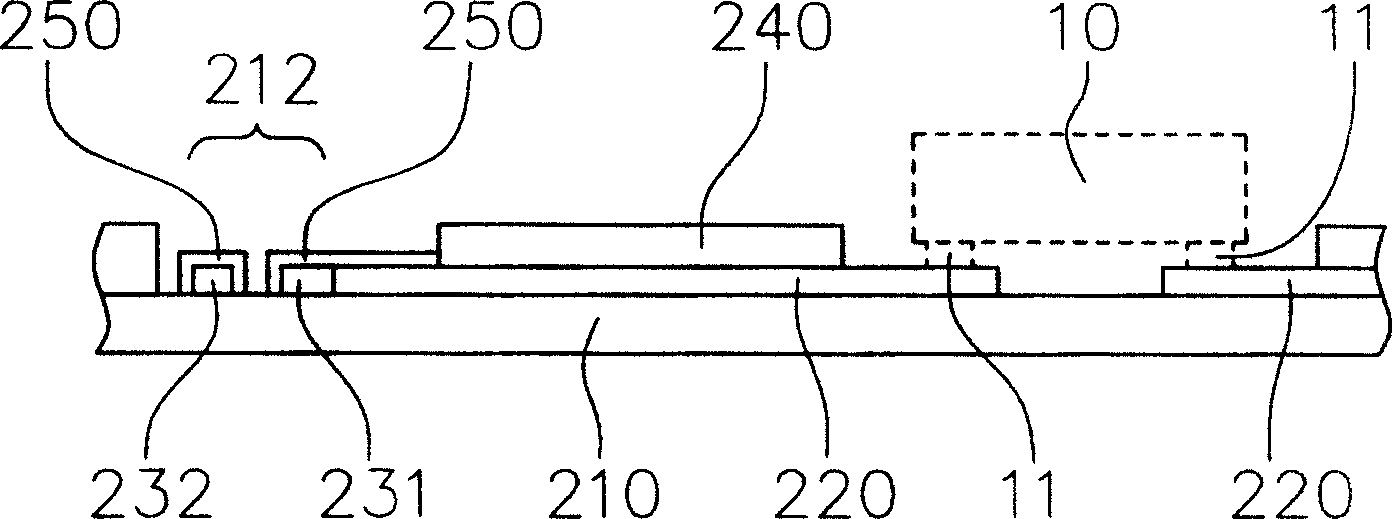
[0059] According to a first embodiment of the present invention, a semiconductor packaging substrate is disclosed. Such as figure 2 and image 3 As shown, the semiconductor package substrate 200 mainly includes a dielectric layer 210 , a plurality of pins 220 , a plurality of first electrostatic guiding lines 231 , a plurality of second electrostatic guiding lines 232 and a solder resist layer 240 . A surface of the dielectric layer 210 defines a plurality of packaging units 211 and a plurality of static dissipative regions 212 . After the packaging process, a semiconductor package structure can be cut out along the periphery of the package units 211 . Generally, these encapsulation units 211 can also be referred to as use areas. The static dissipative area 212 is located between or on the side of the packaging unit 211, and is used to disperse the electrostatic charge of the ground pin or the pin with weak static resistance in these static dissipative areas 212 exposed ou...
PUM
 Abstract
Description
Claims
Application Information
 - R&D
- Intellectual Property
- Life Sciences
- Materials
- Tech Scout
- Unparalleled Data Quality
- Higher Quality Content
- 60% Fewer Hallucinations
Browse by: Latest US Patents, China's latest patents, Technical Efficacy Thesaurus, Application Domain, Technology Topic, Popular Technical Reports.
© 2025 PatSnap. All rights reserved.Legal|Privacy policy|Modern Slavery Act Transparency Statement|Sitemap|About US| Contact US: help@patsnap.com


