Waveguide optical switch and making method thereof

A fabrication method and waveguide light technology, which are applied in the directions of optical waveguides and optical waveguides, coupling of optical waveguides, etc., can solve the problems of high switching driving power, complex fabrication process, large insertion loss, etc., and achieve fast response speed, simple fabrication process, and insertion Low loss effect

Inactive Publication Date: 2008-12-24
CHANGCHUN INST OF OPTICS FINE MECHANICS & PHYSICS CHINESE ACAD OF SCI
View PDF5 Cites 0 Cited by
  • Summary
  • Abstract
  • Description
  • Claims
  • Application Information

AI Technical Summary

Problems solved by technology

Since the lower waveguide is made of silicon dioxide, the upper waveguide is made of polymer, and the vertical coupling layer (common cladding) is made of silicon, the waveguide optical switch has complex manufacturing process, high manufacturing cost, and high switch driving power. Slow response speed, low extinction ratio, large insertion loss, etc.

Method used


Image

  • Waveguide optical switch and making method thereof
  • Waveguide optical switch and making method thereof

Examples


Embodiment Construction

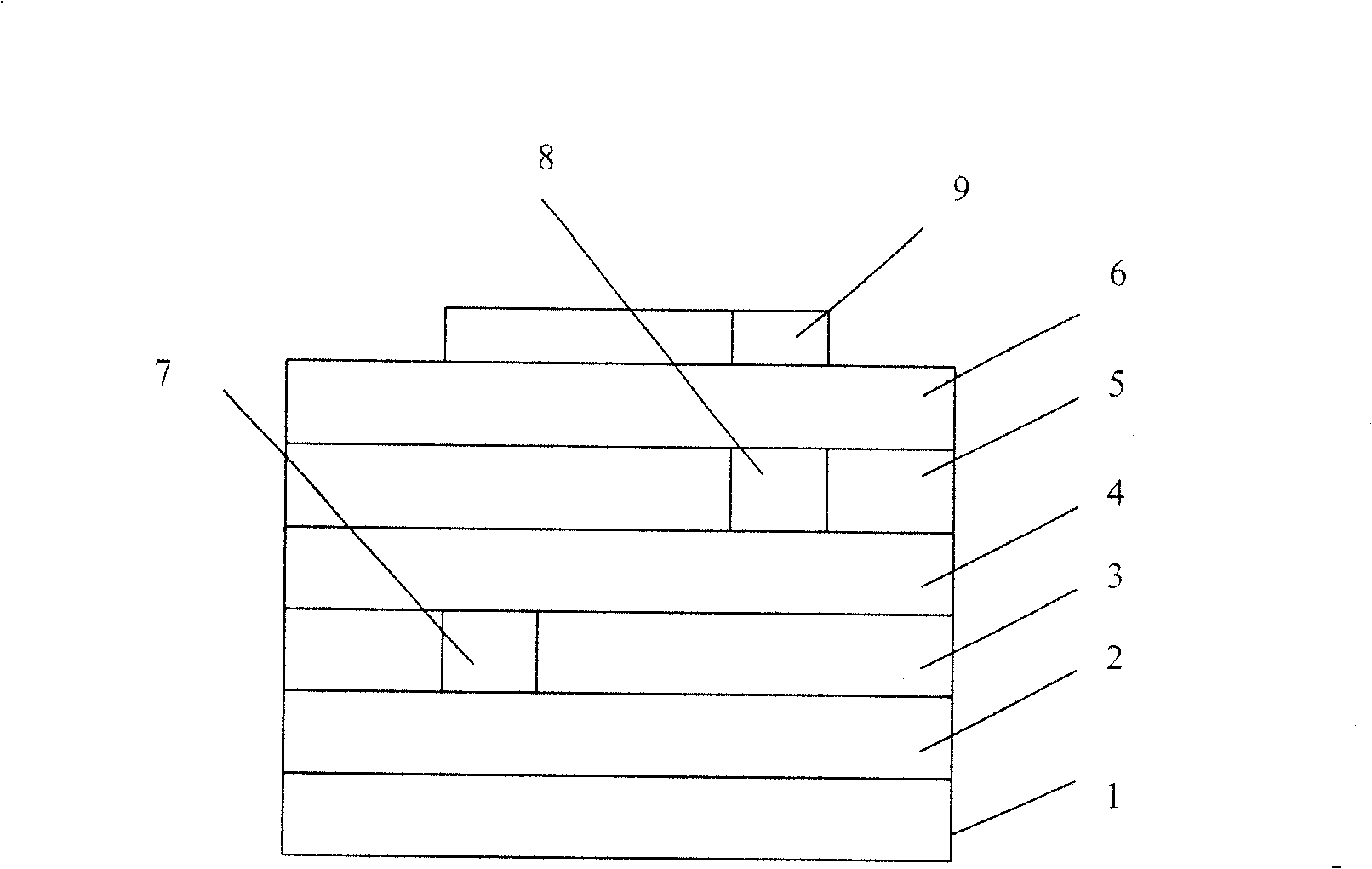
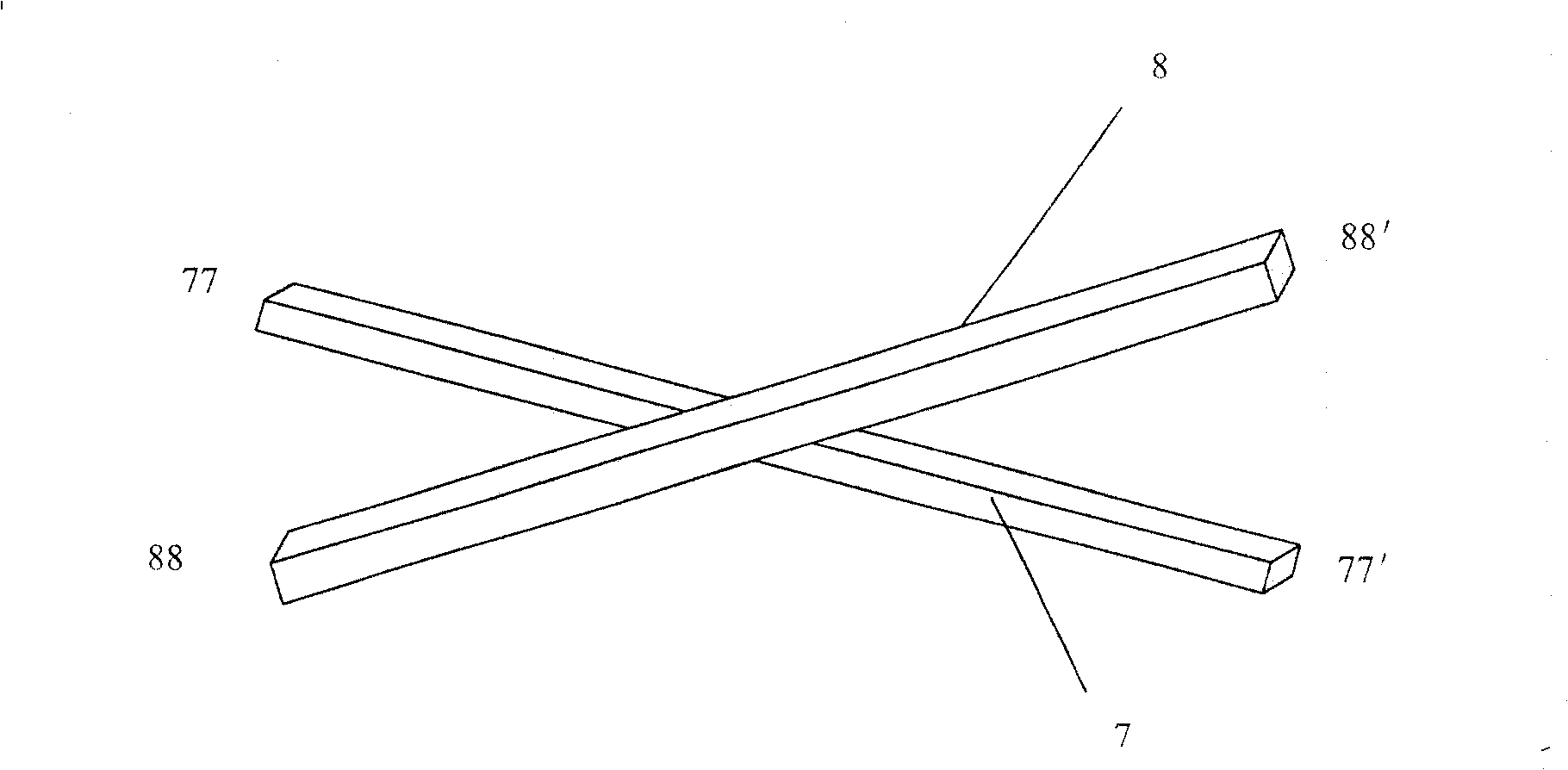
[0023] Such as figure 1 As shown, the present invention adopts a five-layer film structure. From the base silicon chip 1 to the metal electrode 9, the lower waveguide lower cladding layer 2, the lower waveguide core layer, the vertical coupling layer 4 (common cladding layer), the upper waveguide core layer, and the upper waveguide core layer are sequentially formed. Cladding 6 on the waveguide. The base silicon wafer 1 is a high-purity silicon wafer. The lower cladding layer 2 of the lower waveguide is made of polyester polymer BCB, and its thickness can be 3 μm, 4 μm or 5 μm. The thickness of the lower waveguide core layer is 3.6 μm, 3.8 μm, 4.0 μm, or 4.2 μm, including the lower waveguide 7 in this layer and the lower waveguide side cladding 3 around it, and the lower waveguide 7 is made of cyclized rubber polymer Su8 , the lower waveguide side cladding 3 is made of polyester polymer BCB. The vertical coupling layer 4 is made of polyester polymer BCB with a thickness of ...


PUM


Abstract

The invention relates to a 3D vertical coupling type waveguide optical swift and the preparation method thereof; the waveguide optical swift adopts a five-layer film structure which comprises a lower waveguide lower cladding, a lower waveguide sandwich layer, a vertical coupling layer, an upper waveguide sandwich layer and an upper waveguide upper cladding from a base silicon chip to a mental electrode; all of the lower waveguide cladding, the upper waveguide cladding and the vertical coupling layer are made of polyester polymers; an upper waveguide and a lower waveguide are made of cyclized rubber polymers; the upper waveguide and the lower waveguide are in the angle of 0.2 DEG-1.8 DEG.. The five-film structure is prepared by the painting method; the upper waveguide and the lower waveguide are made by photoetching technique. The invention has the advantages of simple manufacture technique, low manufacture cost, low driving power of the swift, rapid response speed, high light extinction ratio and low insertion loss; the waveguide optical swift in the invention can be used in a large scale integration optical waveguide return circuit as a basic unit.

Description

technical field [0001] The invention relates to a waveguide optical switch, in particular to a three-dimensional vertically coupled waveguide optical switch and a manufacturing method thereof. Background technique [0002] Traditional waveguide optical switches are limited to two-dimensional planar integrated structures, which can achieve high precision for microfabrication technology. However, in a waveguide optical switch with a two-dimensional planar structure, the electrode cannot be deposited on the very top of one waveguide, and it is also very close to the other waveguide, so the electrode will affect both waveguides simultaneously, thus requiring a high electrode drive power. [0003] With the development of three-dimensional integrated optics, more and more scientific and technological workers in the field of optoelectronics pay attention to the research of three-dimensional vertically coupled optical waveguide devices. (Keil N, Weinert C, Wirges W, et al.Thermo-o...

Claims


Application Information

Patent Timeline
Patent Type & Authority Patents(China)
IPC IPC(8): G02B6/12G02B6/13G02B6/35
Inventor 鄂书林孔光明赵虎旦邓文渊
Owner CHANGCHUN INST OF OPTICS FINE MECHANICS & PHYSICS CHINESE ACAD OF SCI
Why Eureka
Try Eureka