Method for avoiding or reducing V-defect of blue-green light LED material
A light-emitting diode, blue-green light technology, applied in electrical components, circuits, semiconductor devices, etc., can solve problems such as large lattice mismatch and large difference in thermal expansion coefficient
- Summary
- Abstract
- Description
- Claims
- Application Information
AI Technical Summary
Problems solved by technology
Method used
Image
Examples
Embodiment 1
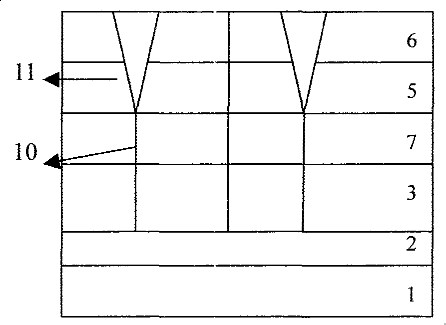
[0029] First, the substrate material sapphire Sapphire substrate layer 1 is desorbed and cleaned for 1 to 10 minutes at a temperature greater than 1100°C in a hydrogen atmosphere;
[0030] Lower the temperature to 500°C, and grow a 25nm-thick low-temperature GaN nucleation layer (low-temperature grown GaN buffer layer 2). During this growth process, the growth pressure is 200 Torr, and the V / III molar ratio is 5000;
[0031] Raise the substrate temperature to 1100°C, anneal the low-temperature GaN nucleation layer in situ, and the annealing time is 1 minute; after annealing, adjust the temperature to 1100°C, and grow a 4 micron n-type doped GaN layer (high temperature The grown layer n-GaN3), the growth pressure is 200Torr, the V / III molar ratio is 3000, and the doping concentration is 1×10 19 cm -3 ;
[0032] Adjust the temperature to a higher temperature region of 1120°C, and control the growth pressure at 75 Torr to grow n-type doped Al x Ga 1-x N / GaN (x=0.2) superlatti...
Embodiment 2
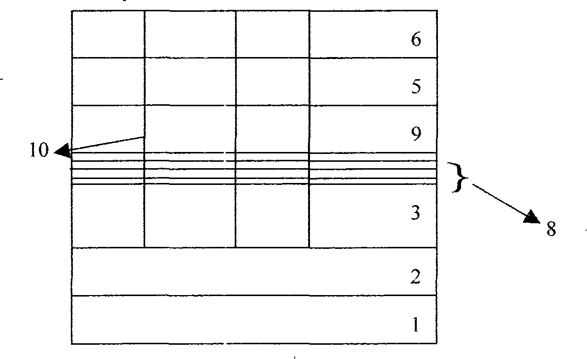
[0039]First, the substrate material sapphire Sapphire substrate layer 1 is desorbed and cleaned for 1 to 10 minutes at a temperature greater than 1100°C in a hydrogen atmosphere;
[0040] Lower the temperature to 500°C, and grow a 25nm-thick low-temperature GaN nucleation layer (low-temperature grown GaN buffer layer 2). During this growth process, the growth pressure is 200 Torr, and the V / III molar ratio is 5000;
[0041] Raise the substrate temperature to 1100°C, anneal the low-temperature GaN nucleation layer in situ, and the annealing time is 1 minute; after annealing, adjust the temperature to 1050°C, and grow a 4 micron n-type doped GaN layer (high temperature The grown layer n-GaN 3), the growth pressure is 200Torr, the V / III molar ratio is 3000, and the doping concentration is 1×10 19 cm -3 ;
[0042] Adjust the temperature to a higher temperature region of 1120°C, and control the growth pressure at 75 Torr to grow n-type doped Al x Ga 1-x N / GaN (x=0.1) superlatti...
Embodiment 3
[0049] First, the substrate material sapphire Sapphire substrate layer 1 is desorbed and cleaned for 1 to 10 minutes at a temperature greater than 1100°C in a hydrogen atmosphere;
[0050] Lower the temperature to 500°C, and grow a 25nm-thick low-temperature GaN nucleation layer (low-temperature grown GaN buffer layer 2). During this growth process, the growth pressure is 200 Torr, and the V / III molar ratio is 5000;
[0051] Raise the substrate temperature to 1100°C, anneal the low-temperature GaN nucleation layer in situ, and the annealing time is 1 minute; after annealing, adjust the temperature to 1050°C, and grow a 4 micron n-type doped GaN layer (high temperature The grown layer n-GaN 3), the growth pressure is 200Torr, the V / III molar ratio is 3000, and the doping concentration is 1×10 19 cm -3 ;
[0052] Adjust the temperature to a higher temperature region of 1120°C, and control the growth pressure at 75 Torr to grow n-type doped Al x Ga 1-x N / GaN (x=0.1) superlatt...
PUM
 Abstract
Description
Claims
Application Information
 - R&D
- Intellectual Property
- Life Sciences
- Materials
- Tech Scout
- Unparalleled Data Quality
- Higher Quality Content
- 60% Fewer Hallucinations
Browse by: Latest US Patents, China's latest patents, Technical Efficacy Thesaurus, Application Domain, Technology Topic, Popular Technical Reports.
© 2025 PatSnap. All rights reserved.Legal|Privacy policy|Modern Slavery Act Transparency Statement|Sitemap|About US| Contact US: help@patsnap.com


